
Eureka
For R&D, Eureka makes reading and utilizing patents & technical documents easy.
Eureka AIR
Designed for self-driven R&D workflows. Generate viable solutions, solve complex R&D challenges, empower your innovation with AI.

Eureka Materials
Designed for material experts only. Revolutionize your material R&D, from search, analyze, to developing new materials.

TechResearch
Generate reliable direction feasibility study reports for your R&D in just a few steps.

TechSeek
Discover and master advanced knowledge NOW. Basics, ideas, possibilities, all at once.

TechMind
As an expert in R&D Theories, TechMind can generates customized viable solutions instantly.

TechRisk
Analyze your overall solution with one click, know your potential R&D risks in advance.

TechMonitor
Get weekly tech updates, stay abreast of the latest tech innovations and key insights.
Coating composition for electric part and process for forming coating film
- Summary
- Abstract
- Description
- Claims
- Application Information
AI Technical Summary
Problems solved by technology
Method used
Image

Examples
example 2
Formation of Transporting Layer for Transistor
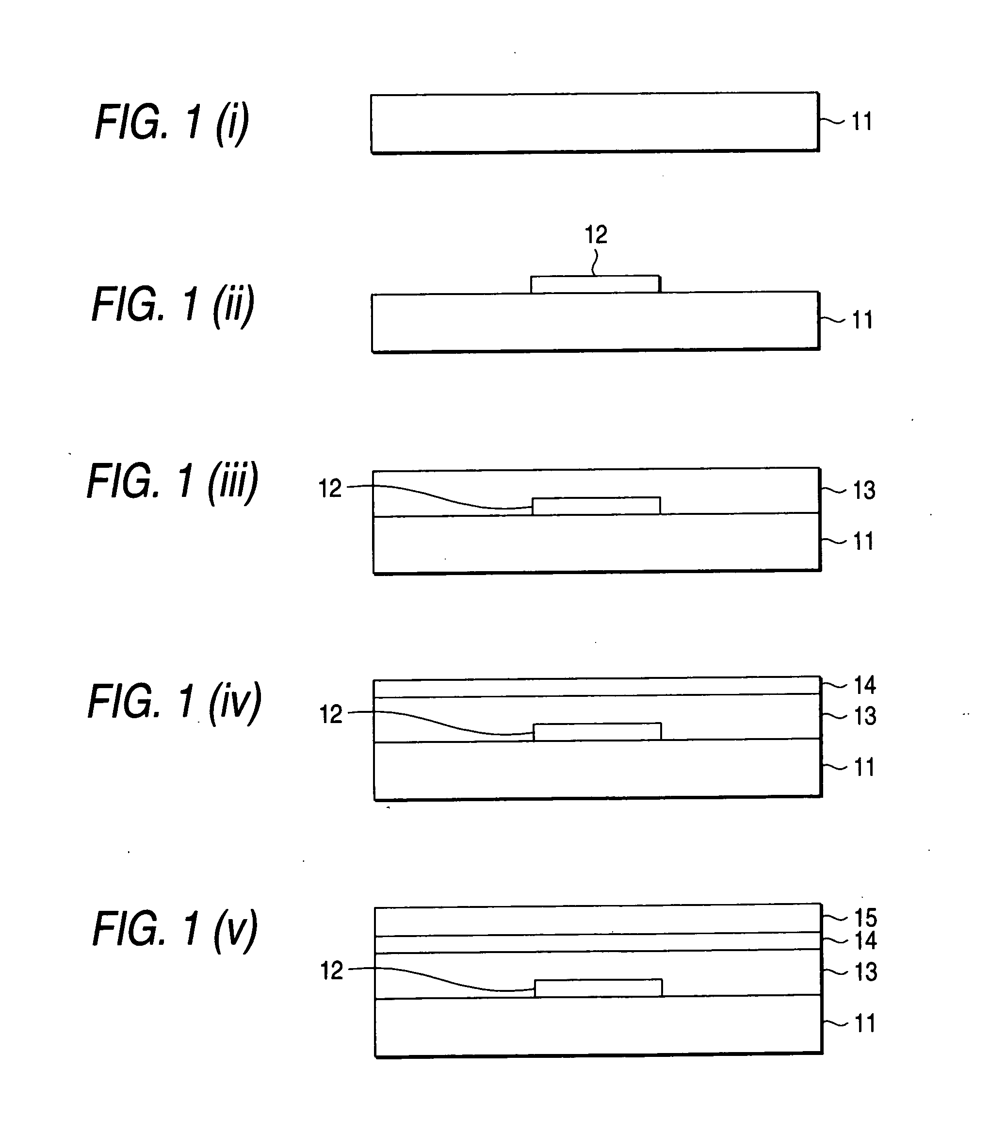
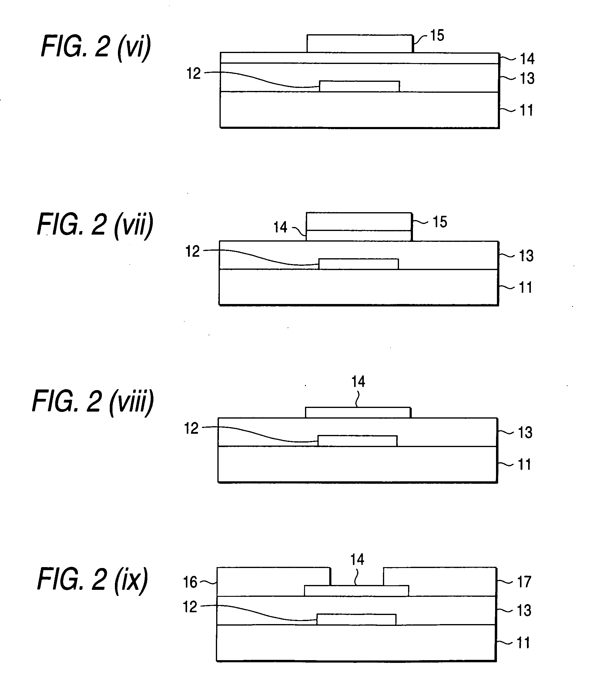
[0127] A MOS type field effect transistor (MOS-FET) having the structure shown in FIGS. 3 and 4 is produced by the production process shown in FIGS. 1-i to 1-v and 2-vi to 2-ix.
[0128] FIGS. 1-i to 1-v and 2-vi to 2-ix are enlarged cross sectional views of a substrate in the process for producing the field effect transistor in Example 2, in which FIGS. 1-i to 1-v show the first half of the process, and FIGS. 2-vi to 2-ix show the last half of the process.
[0129]FIG. 3 is an enlarged plane view of the field effect transistor produced in Example 2, and FIG. 4 is a cross sectional view on line A-A in FIG. 3.
[0130] The operations in Example 2 will be described with reference mainly to FIGS. 1-i to 1-v and 2-vi to 2-ix.
(1) Formation of Coating Film
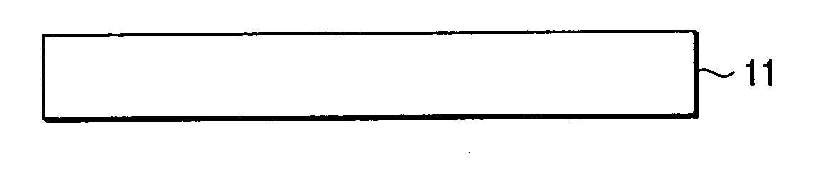
[0131] A silicon wafer 11 as a substrate produced by Advantech Co., Ltd., diameter: 76.2 mm (3 inch), thickness: 380 μm, thickness of surface oxide film: 1 μm) is prepared (FIG. 1-i). A titaniu...
PUM
| Property | Measurement | Unit |
|---|---|---|
| Boiling point | aaaaa | aaaaa |
| Temperature | aaaaa | aaaaa |
| Composition | aaaaa | aaaaa |
Abstract
Description
Claims
Application Information
 - R&D Engineer
- R&D Manager
- IP Professional
- Industry Leading Data Capabilities
- Powerful AI technology
- Patent DNA Extraction
Browse by: Latest US Patents, China's latest patents, Technical Efficacy Thesaurus, Application Domain, Technology Topic, Popular Technical Reports.
© 2024 PatSnap. All rights reserved.Legal|Privacy policy|Modern Slavery Act Transparency Statement|Sitemap|About US| Contact US: help@patsnap.com