Low power sleep mode operation technique for dynamic random access memory (DRAM) devices and integrated circuit devices incorporating embedded DRAM

a dynamic random access memory and low power sleep mode technology, applied in static storage, information storage, digital storage, etc., can solve the problems of not accurately timed when a refresh operation is required over all possible process corners, voltage and temperature, and not sufficiently reducing the transistor leakage power in all circuit blocks, so as to reduce the overall dram power usage, reduce transistor leakage, and reduce the effect of transistor leakag

Active Publication Date: 2005-12-29
SONY CORP
View PDF9 Cites 22 Cited by
  • Summary
  • Abstract
  • Description
  • Claims
  • Application Information

AI Technical Summary

Benefits of technology

[0011] The technique of the present invention further provides for the power-gating “on” and “off” of related row address circuitry. This reduces transistor leakage for the majority of the Sleep Mode operation time and may be effectuated with a boosted power-gate signal level. A delay may be added between the turning “off” of the power-gating signal and the subsequent enabling of the related circuitry such that the internal power supplies have time to achieve the proper supply (VCC) and reference (VSS) levels. Those circuits not related to refresh operation may be kept “off” for the entire

Problems solved by technology

This process is complicated in most instances and a command address latch is used to hold either the externally supplied row address or the internally generated address from the refresh address counter depending on the command.
Despite these technological advances, conventional memory devices, and those incorporating embedded memory, do not accurately time when a re

Method used


Image

  • Low power sleep mode operation technique for dynamic random access memory (DRAM) devices and integrated circuit devices incorporating embedded DRAM
  • Low power sleep mode operation technique for dynamic random access memory (DRAM) devices and integrated circuit devices incorporating embedded DRAM
  • Low power sleep mode operation technique for dynamic random access memory (DRAM) devices and integrated circuit devices incorporating embedded DRAM

Examples


Embodiment Construction

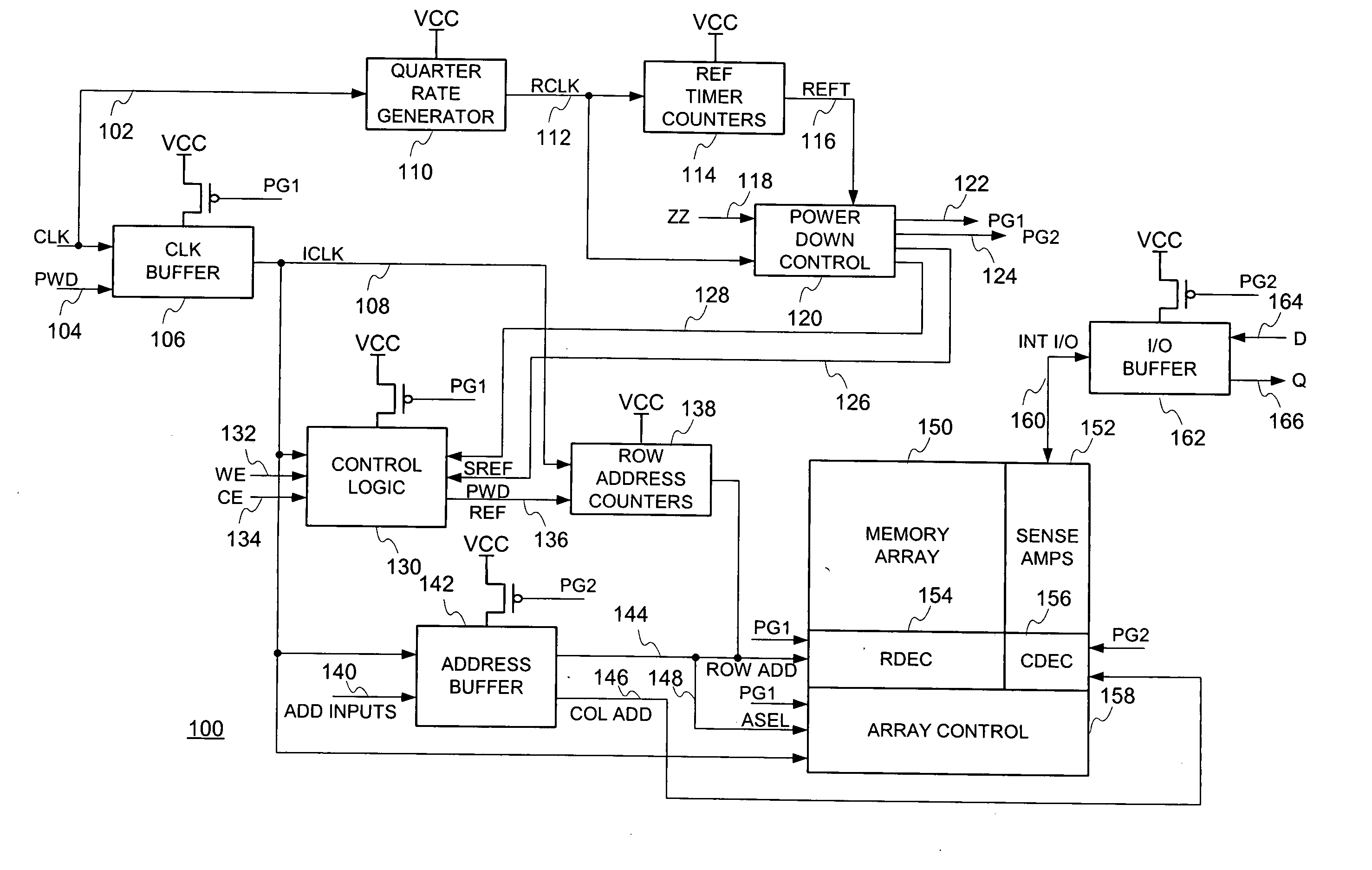
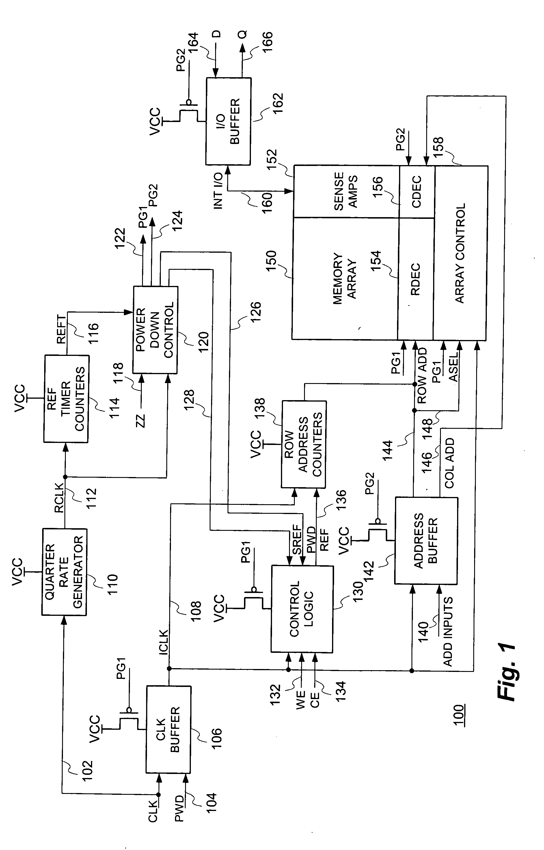
[0020] With reference now to FIG. 1, a functional block diagram of a portion of an integrated circuit device 100 incorporating a memory array and implementing a representative embodiment of the low power Sleep Mode operation technique of the present invention is shown. As will be used herein, the following definitions pertain:

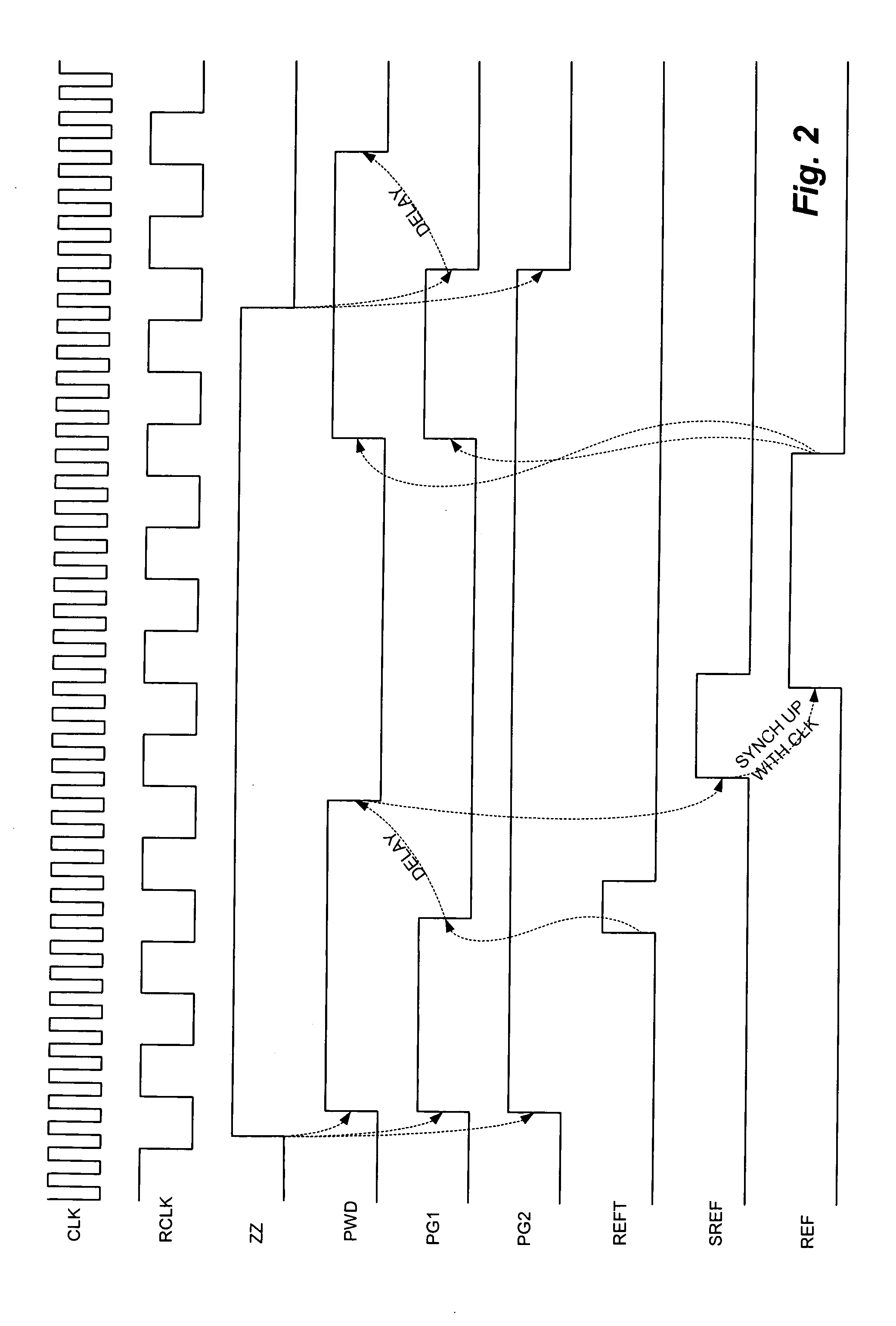
[0021] ClK—the externally applied clock to the embedded DRAM or memory device;

[0022] RCLK—the reduced rate clock which may be ¼th, ⅛th, 1 / 16th or other fraction of the externally applied CLK signal;

[0023] ZZ—the externally applied Sleep Mode command;

[0024] PWD—the power down, enable / disable signal to turn “off” various circuit blocks;

[0025] PG1—the power-gate #1 signal which turns “on” and “off” as required;

[0026] PG2—the power-gate #2 signal which remains “off” for the entire Sleep Mode time;

[0027] REFT—the refresh timer signal which goes “high” when a refresh operation is needed;

[0028] SREF—the start refresh signal which is asserted after the REFT, PG...


PUM


Abstract

A low power Sleep Mode operation technique for dynamic random access (DRAM) devices and integrated circuit devices incorporating embedded DRAM. By counting clock (CLK) cycles in accordance with the technique disclosed, refresh time (tREF) does not vary with all possible process corners, voltages and temperatures (PVT) since the clock signal exhibits a steady frequency over PVT applied to the DRAM and an internal timer placed on chip will vary directly with these parameters. After entering Sleep Mode, the main internal clock signal is inhibited from propagating around the device chip and, at this time, much of the associated circuitry can be power-gated to conserve power, typically with signals that have a boosted level to provide a negative gate-to-source voltage (VGS) on the power-gating transistors.

Description

BACKGROUND OF THE INVENTION [0001] The present invention relates, in general, to the field of integrated circuit (IC) devices. More particularly, the present invention relates to a low power Sleep Mode operation technique for dynamic random access (DRAM) devices and integrated circuit devices incorporating embedded DRAM. [0002] DRAM memory devices incorporate one or more arrays of memory cells, each generally consisting of a single transistor and associated capacitor. The transistor has one terminal coupled to an associated bit line and its gate coupled to a word line. Another terminal is generally coupled to circuit ground through the capacitor and by enabling the transistor via the word line, the charge on the capacitor may be placed on the associated bit line. Due to the dynamic nature of the charge stored in the capacitor, it must be periodically refreshed to replenish the leaked charge. [0003] A “refresh” or “active” command can occur on any clock cycle in an integrated circuit...

Claims


Application Information

Patent Timeline
IPC IPC(8): G11C8/00G11C11/406
CPCG11C5/144G11C11/406G11C2211/4068G11C2211/4067G11C11/40626
Inventor PARRIS, MICHAEL C.JONES, OSCAR FREDERICK JR.BUTLER, DOUGLAS BLAINE
Owner SONY CORP
Why Eureka
Try Eureka