Vertical cavity surface emitting laser diode and process for producing the same

a laser diode and vertical cavity technology, applied in the direction of laser details, semiconductor lasers, electrical devices, etc., can solve the problems of increased divergence angle, difficult to obtain such a vcsel, and inability to achieve excellent production stability of arrays, etc., to achieve small divergence angle, small mode partition noise, and excellent small signal characteristics

Active Publication Date: 2005-12-29
FUJIFILM BUSINESS INNOVATION CORP
View PDF4 Cites 33 Cited by
  • Summary
  • Abstract
  • Description
  • Claims
  • Application Information

AI Technical Summary

Benefits of technology

[0016] The present invention has been made in view of the above circumstances and provides such a vertical cavity surface emitting laser (VCSEL) diode that has a small divergence angle, is excellent in small signal characteristics, has small mode partition noise, and is excellent in production stability, and a process for producing the same.
[0017] In the vertical cavity surface emitting laser diode, a lenticular medium having a downward convex surface is inserted between an upper semiconductor reflector and a metallic part functioning as an upper electrode, so as to provide such a VCSEL that is excellent in large signal characteristics of small mode partition noise as well as in small signal characteristic with good production stability and a small divergence angle.

Problems solved by technology

However, the conventional vertical cavity surface emitting laser diodes have the following problems.
In the case where the lens surface has upward convexity, it is difficult in view of the production process that the interlayer dielectric film and the upper electrode metallic film are produced with uniform thickness and sufficient adhesion strength.
Accordingly, it is difficult to obtain such a VCSEL that has patterns of the interlayer dielectric film and the upper electrode material formed with excellent reproducibility.
Therefore, the structure cannot be excellent in production stability of an array of a VCSEL, which is demanded to have uniformity in coupling efficiency.
Output of all the oscillation modes from a laser can be attained by such a structure that the aperture diameter d1 defined by the upper electrode is equivalent to or larger than the aperture diameter d2 defined by the current confinement structure, but there is a problem that the divergence angle is increased, and the coupling efficiency with an optical fiber is deteriorated.

Method used


Image

  • Vertical cavity surface emitting laser diode and process for producing the same
  • Vertical cavity surface emitting laser diode and process for producing the same
  • Vertical cavity surface emitting laser diode and process for producing the same

Examples


first embodiment

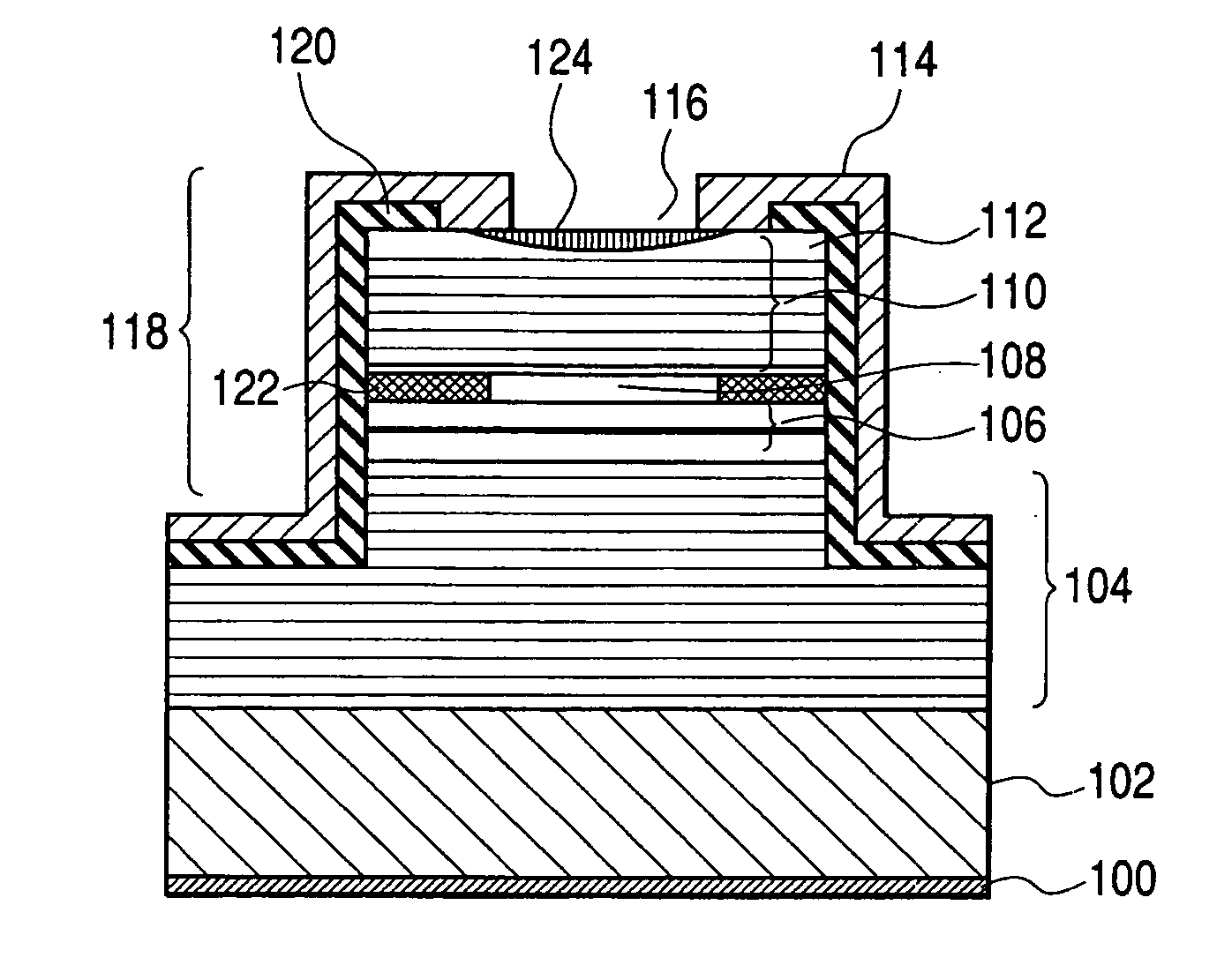
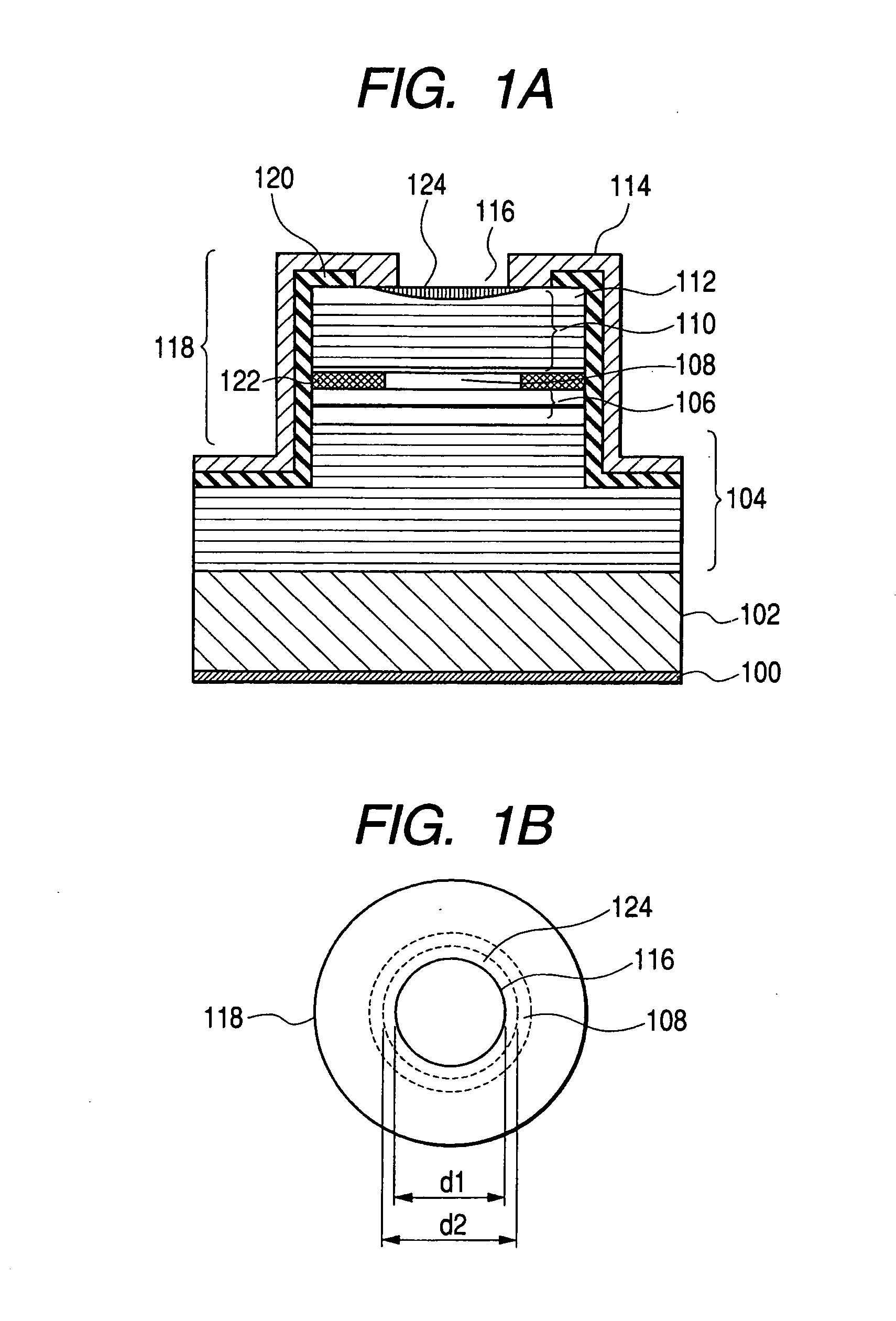
[0050]FIG. 1A is a cross sectional view showing a constitution of a VCSEL according to the invention, and FIG. 1B is a schematic top view showing a VCSEL. As shown in the figures, on a GaAs substrate 102 having an n-side lower electrode 100 formed thereon, semiconductor thin films including an n-type lower semiconductor multi-layer reflector 104, an active region 106, a p-type AlAs layer 108 and a p-type upper semiconductor multi-layer reflector 110 are accumulated in this order. A contact layer 112 formed with p-type GaAs is formed as the uppermost layer of the upper multi-layer reflector 110. A p-side upper electrode 114 is formed on the contact layer 112, and an output aperture 116 having a circular shape is formed at the center of the upper electrode 114. A mesa or post 118 in a cylindrical shape is formed on the substrate up to a part of the lower semiconductor multi-layer reflector 104, and a bottom, a side wall and a part of a top end of the post 118 are covered with an inter...

third embodiment

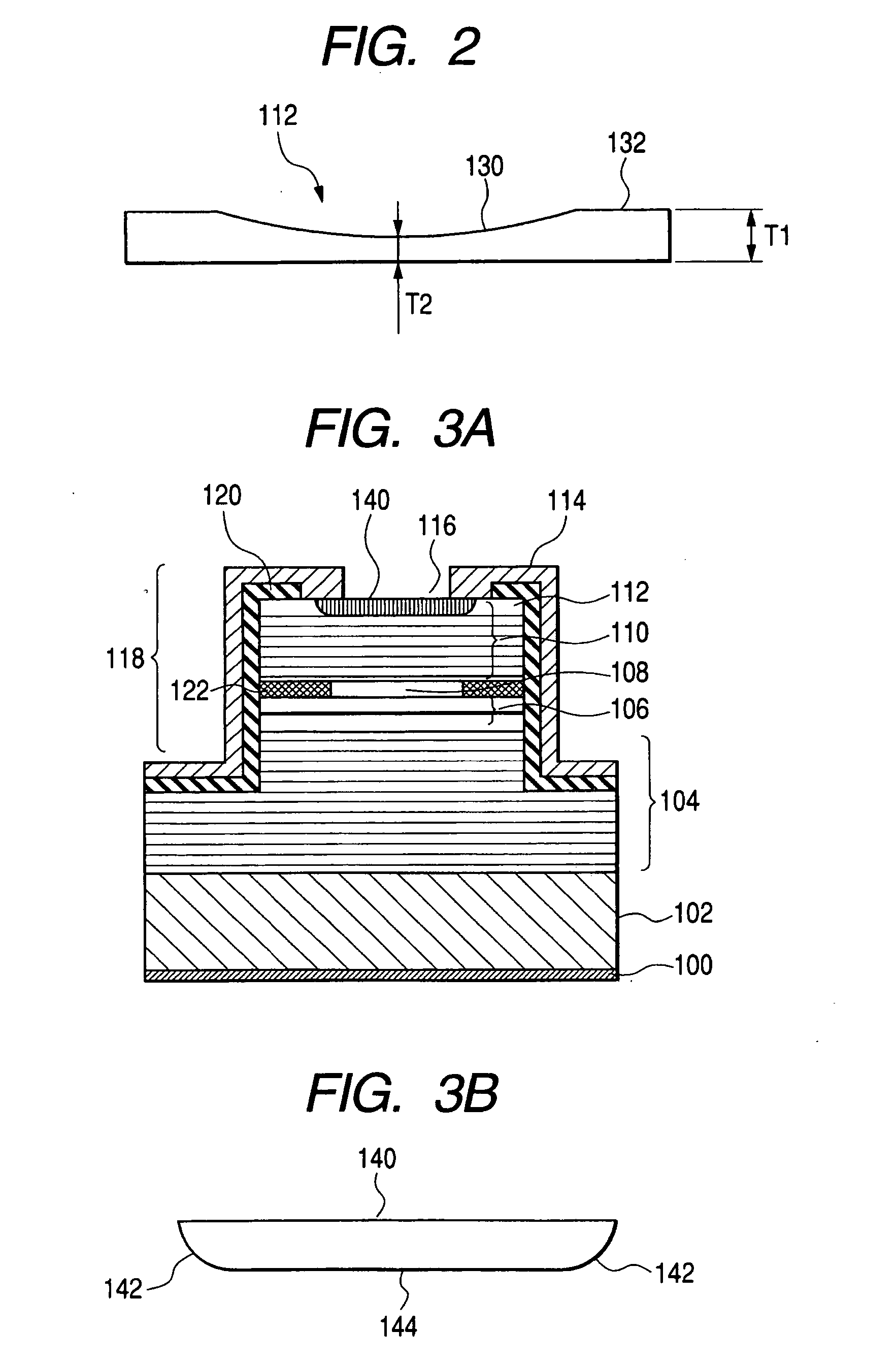
[0080] Subsequently, as shown in FIG. 4, a p-type upper electrode 114 is formed on the top of the post to make electric contact with the contact layer 122. The upper electrode 114 is patterned to form a circular aperture, i.e., the output aperture 116, at the central part thereof. Finally, an n-side electrode 100 is formed on the back surface of the substrate 102 to complete the VCSEL of the

[0081] A fifth embodiment of the invention will be described. The fifth embodiment relates to a process for producing the VCSEL of the second embodiment. As similar to the case of the fourth embodiment, a lower semiconductor multi-layer reflector 104, an active region 106, an AlAs layer 108, an upper semiconductor multi-layer reflector 110, an etching stop layer 152 and a contact layer 112 are accumulated on a semiconductor substrate 102. In the fifth embodiment, the etching stop layer 152 is formed with AlAs as being different from the fourth embodiment.

[0082] The substrate having the plural se...

fourth embodiment

[0083] The subsequent process steps are carried out in the same manner as in the fourth embodiment, and a VCSEL equipped with a lenticular medium having a curved surface only on the peripheral part can be finally obtained.


PUM


Abstract

A vertical cavity surface emitting laser diode includes a lower semiconductor reflector, an active region, an upper semiconductor reflector constituting a resonator with the lower semiconductor reflector, a metallic part being formed on the upper semiconductor reflector, which has a first aperture defining an output region of laser light generated in the active region, and a light confining region being provided between the metallic part and the lower semiconductor reflector, and having a second aperture defining an emission region of the laser light. The upper semiconductor reflector includes a lenticular medium having a convex surface toward the lower semiconductor reflector.

Description

[0001] This application is a continuation-in-part of application Ser. No. 11 / 009,057 entitled “Vertical cavity surface emitting laser diode and process for producing the same” filed Dec. 13, 2004, inventors Naotaka Mukoyama and Nobuaki Ueki.BACKGROUND OF THE INVENTION [0002] 1. Field of the Invention [0003] The present invention relates to a vertical cavity surface emitting laser diode, and more particularly, it relates to a vertical cavity surface emitting laser diode used as a light source for optical information processing and optical communication and a light source for a data storage device storing data with light. [0004] 2. Description of the Related Art [0005] A vertical cavity surface emitting laser diode (hereinafter, referred to as VCSEL) is a laser diode that emits light from a surface of a semiconductor substrate and has such characteristic features as (1) a low driving voltage, (2) capability of wafer level characteristic examination and (3) easiness in implementation, ...

Claims


Application Information

Patent Timeline
Patent Type & Authority Applications(United States)
IPC IPC(8): H01S5/00H01S5/022H01S5/042H01S5/183H01S5/42
CPCH01S5/005H01S5/02284H01S5/02288H01S2301/18H01S5/18311H01S5/18388H01S5/423H01S5/0421H01S5/02251H01S5/02253H01S5/183
Inventor MUKOYAMA, NAOTAKAUEKI, NOBUAKI
Owner FUJIFILM BUSINESS INNOVATION CORP
Why Eureka
Try Eureka