Iridium compound and organic electroluminescent device using the same
a technology of organic electroluminescent devices and compound compounds, which is applied in the direction of indium organic compounds, other domestic articles, natural mineral layered products, etc., can solve the problems of limited emission efficiency, low emission efficiency and lifetime characteristics of blue phosphorescent materials, and lack of suitable host materials for blue phosphorescent materials. , to achieve the effect of low power consumption and high color purity
- Summary
- Abstract
- Description
- Claims
- Application Information
AI Technical Summary
Benefits of technology
Problems solved by technology
Method used
Image
Examples
synthesis example 1
Compound Represented by Formula 2
[0061] A compound represented by formula 2 was synthesized according to the following scheme 2:
[0062] Synthesis of Intermediate (A)
[0063] 6.0 mL (12.0 mmol) of lithium diisopropylamide (LDA) was dropwise added to a solution of 1.4 g (10.0 mmol) of difluorobenzonitrile in 50 mL of diethyl ether at −78° C. and stirred for one hour. Then, 12.5 mL (12.5 mmol) of a 1M trimethyltin chloride solution was added to the reaction mixture and stirred at room temperature for one hour.
[0064] After the reaction was terminated, 20 mL of a 5% sodium hydroxide aqueous solution was added to the reaction solution and the aqueous layer was neutralized with a 3N HCl solution. The resultant solution was separated into an aqueous layer and an organic layer to isolate the organic layer. The aqueous layer was three times extracted with 20 mL of ethyl acetate, and collected organic layers were dried over magnesium sulfate then evaporated to dryness. The resultant residue ...
synthesis example 2
Compound of Formula 3
[0075] A compound of formula 3 was synthesized according to the following scheme 3:
[0076] Synthesis of Intermediate (B-2)
[0077] 1.08 mg (3.6 mmol) of the intermediate (A) and 366 mg (3.0 mmol) of 2-bromo-4-dimethylaminopyridine were dissolved in 18 mL of DMF. Then, 200 mg (0.18 mmol) of palladium tetrakistriphenylphosphine and 2.48 g (17.9 mmol) of K2CO3 were added and the resultant solution stirred at 120° C. for one hour.
[0078] The reaction solution was extracted three times with ethyl ether (10 mL for each). The organic layer was collected and was dried over magnesium sulfate to evaporate a solvent. The resultant residue was purified by silica gel column chromatography to give 715 mg (yield: 92%) of a compound (B-2), which was identified by 1H NMR.
[0079]1H NMR (CDCl3, 400 MHz) δ (ppm) 8.31-8.25 (m, 2H), 7.16 (m, 1H), 6.98 (s, 1H), 6.54 (m, 1H), 3.07 (s, 6H)
[0080] Synthesis of Intermediate (C-2)
[0081] 2.0 g (7.71 mmol) of the intermediate (B-2) was dis...
example 1
Fabrication of Organic EL Device
[0091] A Corning 15 Ω / cm2 (1,200 Å) ITO glass substrate was cut into pieces of 50 mm×50 mm×0.7 mm in size, followed by ultrasonic cleaning in isopropyl alcohol and deionized water (5 minutes for each) and then UV / ozone cleaning (30 minutes), to be used as an anode.
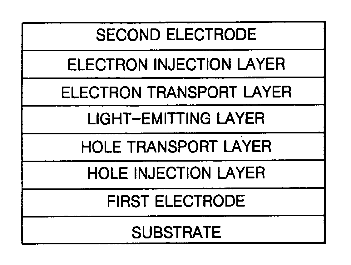
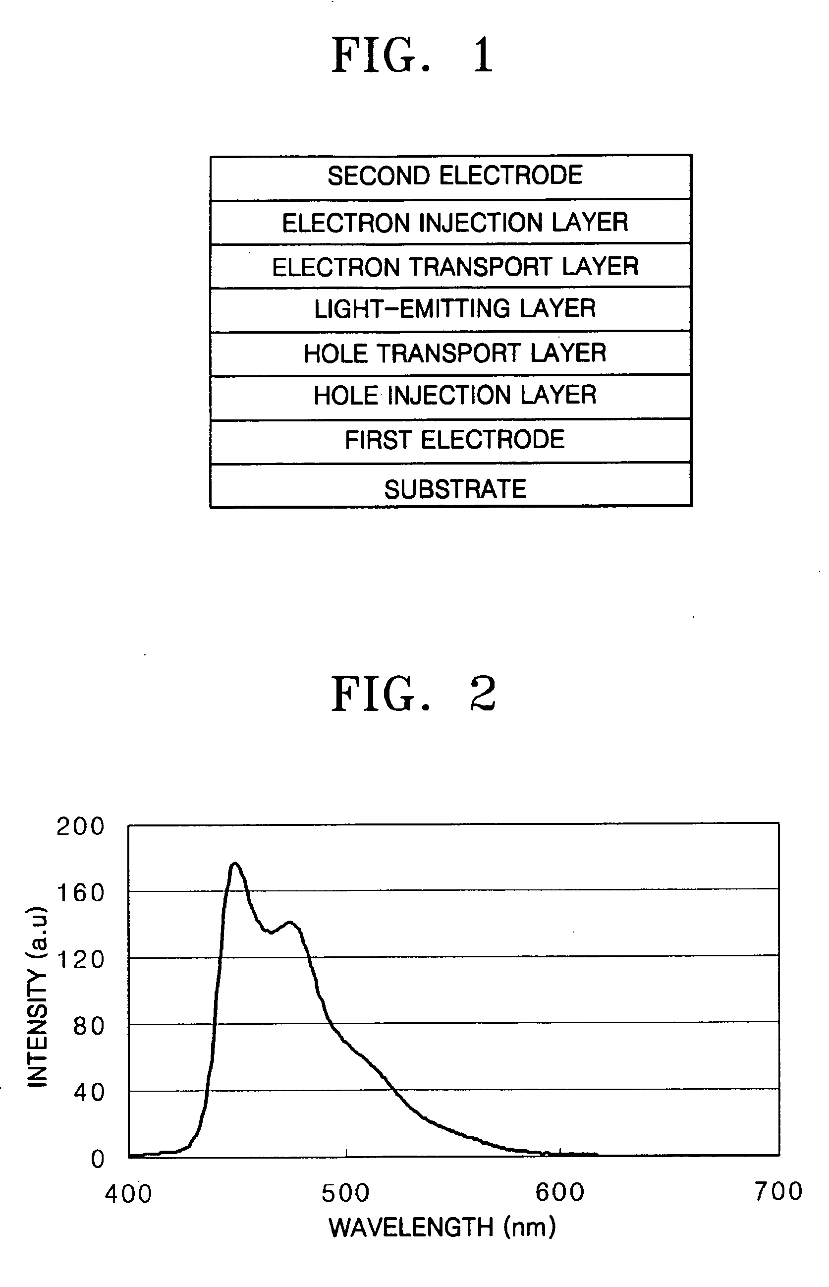
[0092] A hole injection layer was formed to a thickness of 600 Å on the substrate by vacuum deposition of IDE406 (Idemitsu). Then, a hole transport layer was formed to a thickness of 300 Å on the hole injection layer by vacuum deposition of IDE320 (Idemitsu). After forming the hole transport layer, a light-emitting layer was formed to a thickness of 300 Å on the hole transport layer by vacuum co-deposition of 90 parts by weight of SDI-BH-23 as a host and 10 parts by weight of a compound of the formula 2 as a dopant.
[0093] Next, a hole blocking layer was formed to a thickness of 50 Å on the light-emitting layer by vacuum deposition of Balq. Then, an electron transport layer was formed to a...
PUM
| Property | Measurement | Unit |
|---|---|---|
| internal quantum efficiency | aaaaa | aaaaa |
| internal quantum efficiency | aaaaa | aaaaa |
| internal quantum efficiency | aaaaa | aaaaa |
Abstract
Description
Claims
Application Information


