Dual-frequency silicon nitride for spacer application

a technology of silicon nitride and spacer, which is applied in the manufacture of semiconductor/solid-state devices, electrical equipment, basic electric elements, etc., can solve the problems of uneven thickness, serious conformality problems of pecvd film, and temperature used in rtcvd processing, etc., and achieve good conformality

Inactive Publication Date: 2005-12-29
IBM CORP
View PDF7 Cites 24 Cited by
  • Summary
  • Abstract
  • Description
  • Claims
  • Application Information

AI Technical Summary

Benefits of technology

[0007] In view of the foregoing, it is an objective of the present invention to provide a low-temperature method for forming a silicon nitride layer that has good conformality.

Problems solved by technology

However, the temperatures used in RTCVD processing may still exceed the thermal budget for the device.
However, the conventional technique of using a PECVD film suffers from a serious conformality problem, that is, the film is uniform when deposited on near-planar substrate features but has uneven thickness when features with different aspect ratio are present.
The two big problems for PECVD silicon nitride films for spacer applications is the poor conformality (less than 50%) and the presence of seams 43 (which may be observed from subsequent wet cleans that are used to form cobalt silicide junction contacts to the source-drain regions).

Method used


Image

  • Dual-frequency silicon nitride for spacer application
  • Dual-frequency silicon nitride for spacer application
  • Dual-frequency silicon nitride for spacer application

Examples


Embodiment Construction

[0023] In the following description, numerous specific details may be set forth to provide a thorough understanding of the present invention. However, it will be obvious to those skilled in the art that the present invention may be practiced without such specific details.

[0024] Refer now to the drawings wherein depicted elements are not necessarily shown to scale and wherein like or similar elements are designated by the same reference numeral through the several views.

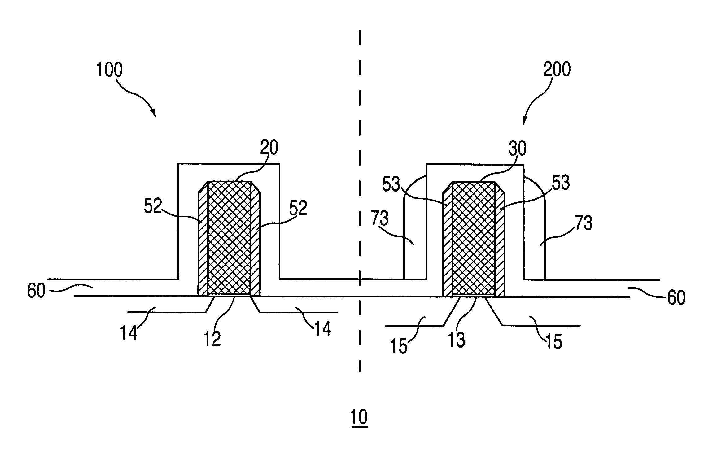
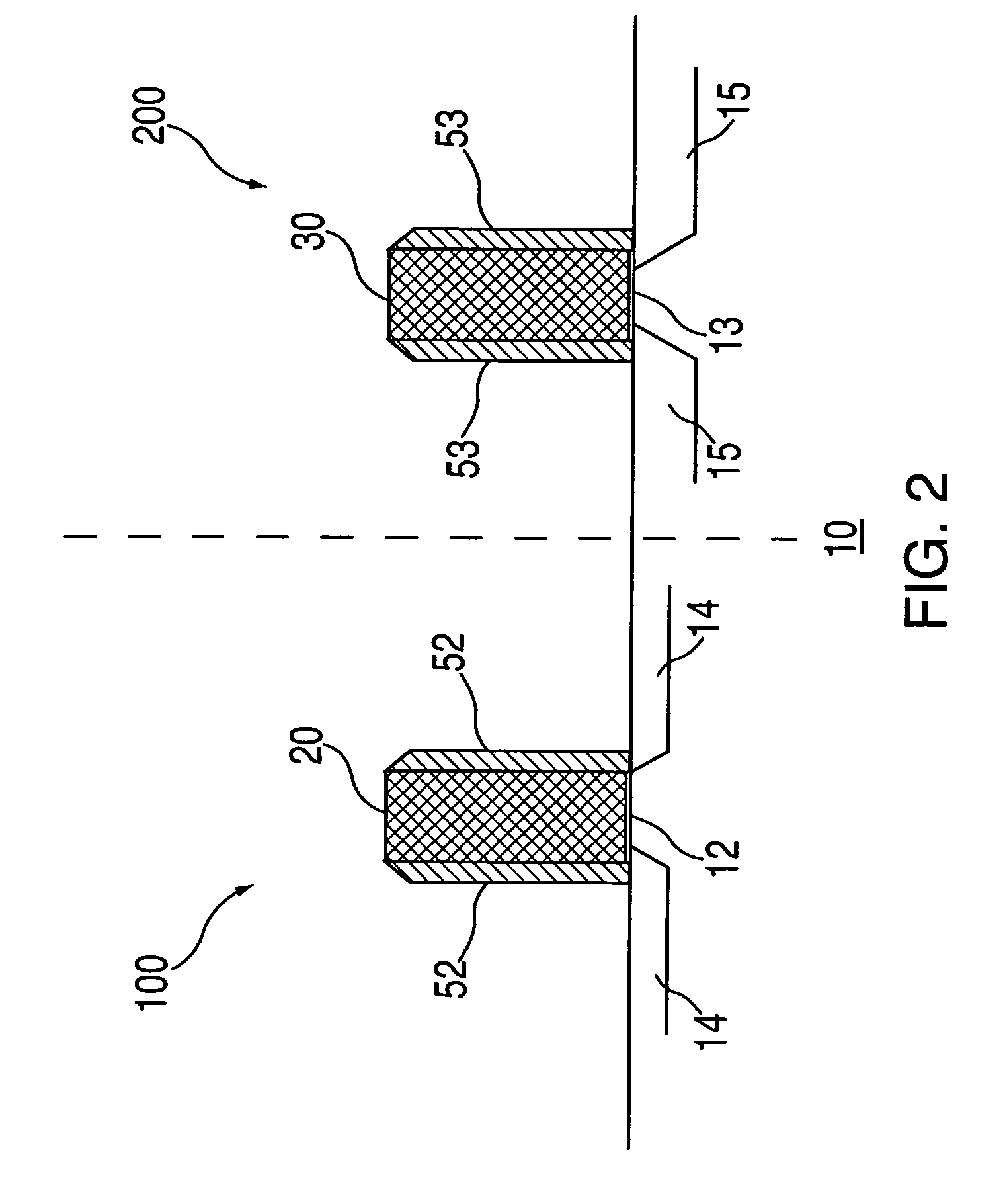
[0025]FIG. 2 shows two gate stacks 20, 30 formed by techniques known in the art on the same semiconductor substrate 10 in an NFET region 100 and a PFET region 200 respectively. The gate stacks may be comprised of a polysilicon conductor, having width typically between about 300 Å to 800 Å, and the height of the poly line is typically on the order of 1000 Å to 2000 Å. The substrate may be a bulk wafer, SOI wafer, GaAs or any type of semiconductor substrate. A gate oxide layer 12, 13 may be present under the gate stac...


PUM

PropertyMeasurementUnit
temperatureaaaaaaaaaa
pressureaaaaaaaaaa
temperatureaaaaaaaaaa

Abstract

A silicon nitride spacer material for use in forming a PFET device and a method for making the spacer includes the use of a dual-frequency plasma enhanced CVD process wherein the temperature is in the range depositing a silicon nitride layer by means of a low-temperature dual-frequency plasma enhanced CVD process, at a temperature in the range 400° C. to 550° C. The process pressure is in the range 2 Torr to 5 Torr. The low frequency power is in the range 0 W to 50 W, and the high frequency power is in the range 90 W to 110 W. The precursor gases of silane, ammonia and nitrogen flow at flow rates in the ratio 240:3200:4000 sccm. The use of the silicon nitride spacer of the invention to form a PFET device having a dual spacer results in a 10%-15% performance improvement compared to a similar PFET device having a silicon nitride spacer formed by a RTCVD process.

Description

BACKGROUND OF INVENTION [0001] The present invention relates in general to the manufacture of integrated circuits, and in particular relates to spacer films used in semiconductor devices. [0002] Semiconductor devices such as a metal oxide semiconductor field effect transistors (MOSFETs) are known in the art. P-type FETs (PFETs) or n-type FETs (NFETs) are often formed using very different dopant species. These species have very different physical properties such as diffusion rate and maximum activated concentration. A spacer is used to define the edge for the source-drain implants for a FET device. When a voltage is applied at the gate and the channel under the gate oxide is active, there is flow of electrical carriers from the source to the drain. [0003] The use of dual spacers has been described, for example by Fung et al. (co-assigned U.S. patent application Ser. No. 10 / 277,907, filed on Oct. 21, 2002, to the same assignee as the present application), which is incorporated by refe...

Claims


Application Information

Patent Timeline
Patent Type & Authority Applications(United States)
IPC IPC(8): H01L21/31H01L21/318H01L21/44H01L21/8234H01L21/8238
CPCH01L21/823864H01L21/3185H01L21/0217H01L21/02274
Inventor RAMACHANDRAN, RAVIKUMARKELLIHER, JAMES T.NARASIMHA, SHREESHSLEIGHT, JEFFREY W.
Owner IBM CORP
Why Eureka
Try Eureka