Capacitor of a memory device and fabrication method thereof

a memory device and capacitor technology, applied in the direction of capacitors, semiconductor devices, electrical devices, etc., can solve the problems of reducing the integration area of the capacitor, affecting the stability of the step coverage, and deteriorating the ferroelectric properties of the capacitor, so as to improve the fatigue characteristics, reduce production costs, and increase the capacitance and integration

Inactive Publication Date: 2006-01-05
SAMSUNG ELECTRONICS CO LTD
View PDF99 Cites 28 Cited by
  • Summary
  • Abstract
  • Description
  • Claims
  • Application Information

AI Technical Summary

Benefits of technology

[0018] It is another feature of an embodiment of the present invention to provide a vertical stack-type capacitor of a memory device, and method of forming the same, having improved fatigue characteristics.
[0019] It is yet another feature of an embodiment of the present invention to provide a vertical stack-type capacitor of a memory device, and method of forming the same, that reduces production costs.
[0020] It is still another feature of an embodiment of the present invention to provide a vertical stack-type capacitor of a memory device, and method of forming the same, which increases capacitance and integration.

Problems solved by technology

However, when using a planar capacitor structure, increasing the capacitor's area limits integration of a semiconductor device.
Thus, if a ferroelectric thin film is deposited on the metal oxide electrode, the metal oxide electrode may react with the ferroelectric thin film, deteriorating its ferroelectric properties.
Thus, stable step coverage is difficult to achieve during the formation of the ferroelectric thin film.
When depositing a typical ferroelectric material such as lead zirconate titanate (PZT) or barium strontium titanate (BST) on a lower electrode in the opening having a high aspect ratio using chemical vapor deposition (CVD), it is almost impossible to achieve step coverage at temperatures higher than about 500° C.
However, the stack type capacitor structure, which is fabricated by forming a lower electrode and etching the lower electrode as shown in FIG. 1B, also has many problems in its actual manufacturing process, as explained in detail below.
As a result, the unit cell area of a memory device also increases, thereby decreasing integration.
Second, production is expensive.
However, considering the cost of the precious metal used in the lower electrode 14, such a thick lower electrode 14 is not desirable.
Additionally, the time for deposition and etching of the lower electrode 14 is lengthened, further increasing the production cost.
Third, the stack type capacitor formed by etching may not improve fatigue characteristics of the metal oxide electrode.
However, the metal oxide electrode on the lateral side of the lower electrode is not perpendicular to the electric field, thereby deteriorating fatigue characteristics.

Method used


Image

  • Capacitor of a memory device and fabrication method thereof
  • Capacitor of a memory device and fabrication method thereof
  • Capacitor of a memory device and fabrication method thereof

Examples


first embodiment

[0035] A capacitor of a memory device according to the present invention is then formed on the lower structure described above. A lower electrode 30 including a metal electrode 36 and a metal oxide electrode 35 is formed on an oxidation stop layer 31. In the particular example shown, the lower electrode 30 has a cylindrical shape. A ferroelectric layer 37 and an upper electrode 38 are sequentially formed and surround, i.e., cover a top surface and lateral surfaces, the lower electrode 30.

[0036]FIG. 2B illustrates a cross-sectional view of a capacitor of a memory device according to a second embodiment of the present invention. Referring to FIG. 2B, a capacitor of the second embodiment of the present invention is formed on a lower structure including a transistor structure. The transistor structure shown in FIG. 2B is identical to the conventional lower structure shown in FIG. 2A, and will not be described again in detail. Again, the transistor structure shown in FIG. 2B includes the...

second embodiment

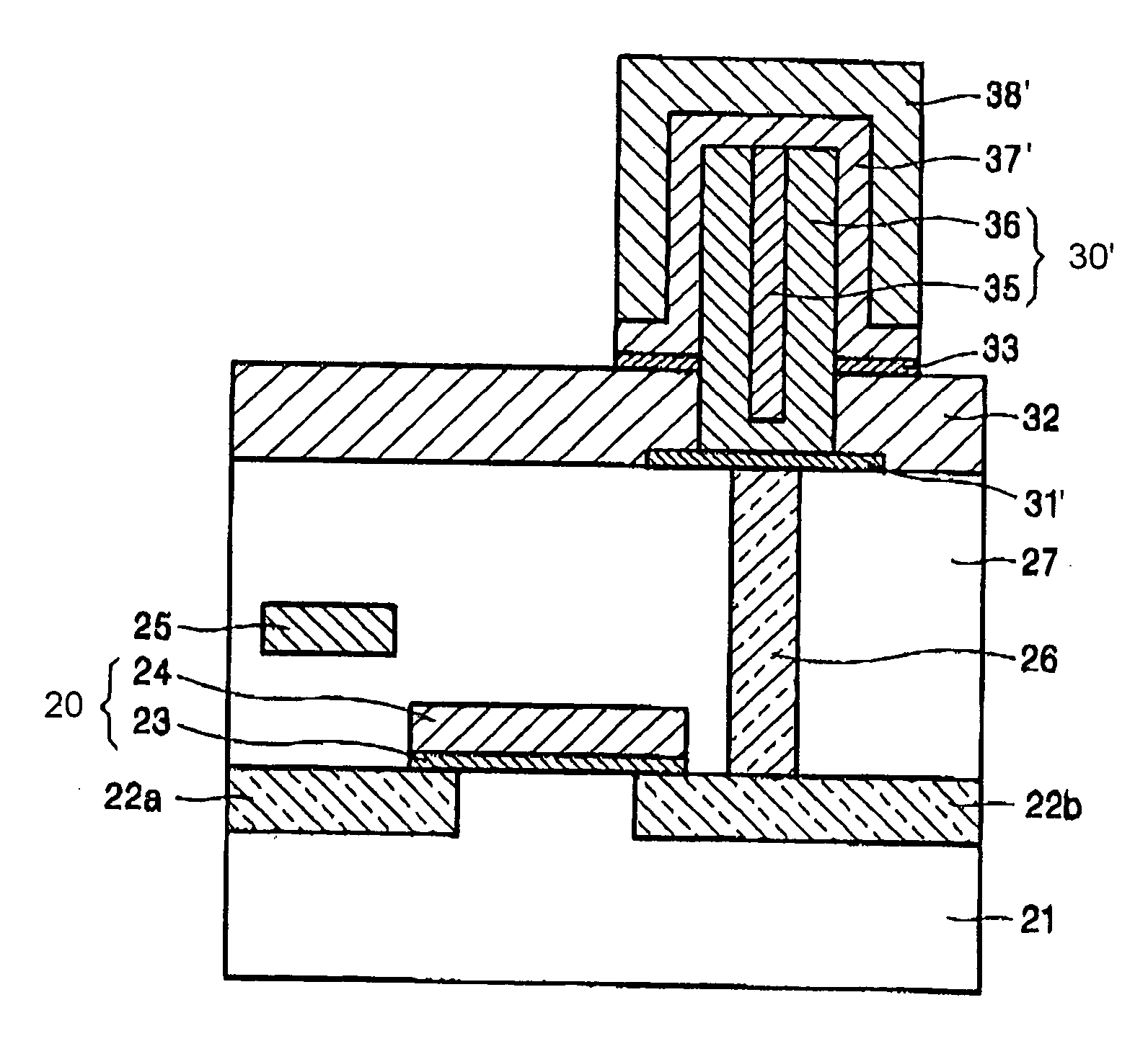
[0037] A capacitor of a memory device according to the present invention is formed on the lower structure described above. A lower electrode 30′ had a cylindrical shape, and includes a metal electrode 36′ and a metal oxide electrode 35′ formed on an oxidation stop layer 31′. An insulating layer 32 and an adhesion layer 33 are formed on the oxidation stop layer 31′ and surround a lower lateral portion of the lower electrode 30′. A ferroelectric layer 37′ and an upper electrode 38′ are sequentially formed on the adhesion layer 33, and cover the top surface and the remaining lateral surface of the lower electrode 30′.

[0038] The capacitor of a memory device according to the second embodiment of the present invention differs from that of the first embodiment in the inclusion of the insulating layer 32 which supports the lateral sides of the lower electrode 30′. This support is especially advantageous when the lower electrode 30′ has a high aspect ratio. When the lower electrode 30′ has a...


PUM

PropertyMeasurementUnit
temperaturesaaaaaaaaaa
angleaaaaaaaaaa
thicknessaaaaaaaaaa

Abstract

A capacitor of a memory device, and a method of fabricating the same, includes a lower electrode electrically coupled to a doping region of a transistor structure, the lower electrode having a metal electrode and a metal oxide electrode, a ferroelectric layer covering and extending laterally along the lower electrode, and an upper electrode formed on the ferroelectric layer.

Description

BACKGROUND OF THE INVENTION [0001] 1. Field of the Invention [0002] The present invention relates to a capacitor of a memory device and a fabrication method thereof. More particularly, the present invention relates to a capacitor of a memory device having a vertical metal electrode / metal oxide electrode and a method of fabricating the same. [0003] 2. Description of the Related Art [0004] A ferroelectric random access memory (FRAM) is a nonvolatile memory device that may be used in computers, MP3 players, digital cameras, personal digital assistants (PDAs), and other electronic devices. The capacitance of a ferroelectric capacitor per unit area should be increased in order to provide a highly-integrated ferroelectric memory device, which includes one transistor and one capacitor. [0005] For a given dielectric material, a capacitor's area may be increased in order to increase its capacitance C, as given by Equation (1) below. C=εA / t  (1) where ε is the permittivity, A is the effectiv...

Claims


Application Information

Patent Timeline
Patent Type & Authority Applications(United States)
IPC IPC(8): H01L21/00H01L27/108H01L21/02H01L27/105H01L21/8246H01L27/10H01L27/115
CPCH01L27/11502H01L27/11507H01L28/91H01L28/65H01L28/55H10B53/30H10B53/00H01L27/105
Inventor PARK, YOUNG-SOOLEE, JUNG-HYUNCHO, CHOONG-RAEKOO, JUNE-MOKIM, SUK-PILSHIN, SANG-MIN
Owner SAMSUNG ELECTRONICS CO LTD
Why Eureka
Try Eureka