

Bird's beak-less or STI- less OTP EPROM
a technology of eprom and eprom layer, which is applied in the direction of semiconductor devices, electrical devices, transistors, etc., can solve the problems of weak or otherwise unreliable memory cells, non-uniform local thinning in the subsequent growth of gate oxide layers, and cell charge loss, so as to facilitate the fabrication of more reliable otp memory cells, reduce wafer manufacturing costs, and uniform gate oxide thickness
- Summary
- Abstract
- Description
- Claims
- Application Information
AI Technical Summary
Benefits of technology
Problems solved by technology
Method used
Image

Examples
Embodiment Construction
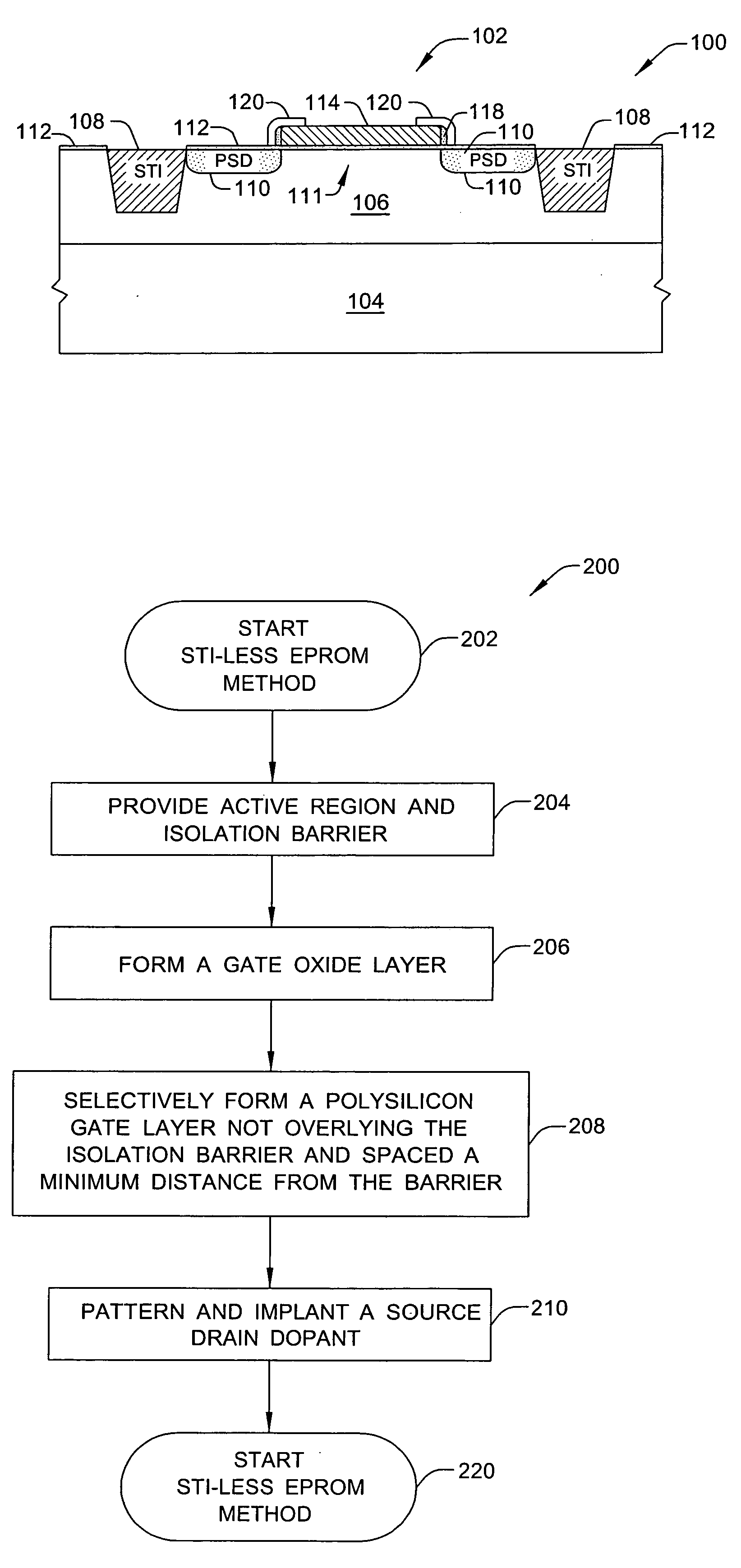
[0025] The present invention will now be described with respect to the accompanying drawings in which like numbered elements represent like parts. The figures provided herewith and the accompanying description of the figures are merely provided for illustrative purposes. One of ordinary skill in the art should realize, based on the instant description, other implementations and methods for fabricating the devices and structures illustrated in the figures and in the following description.
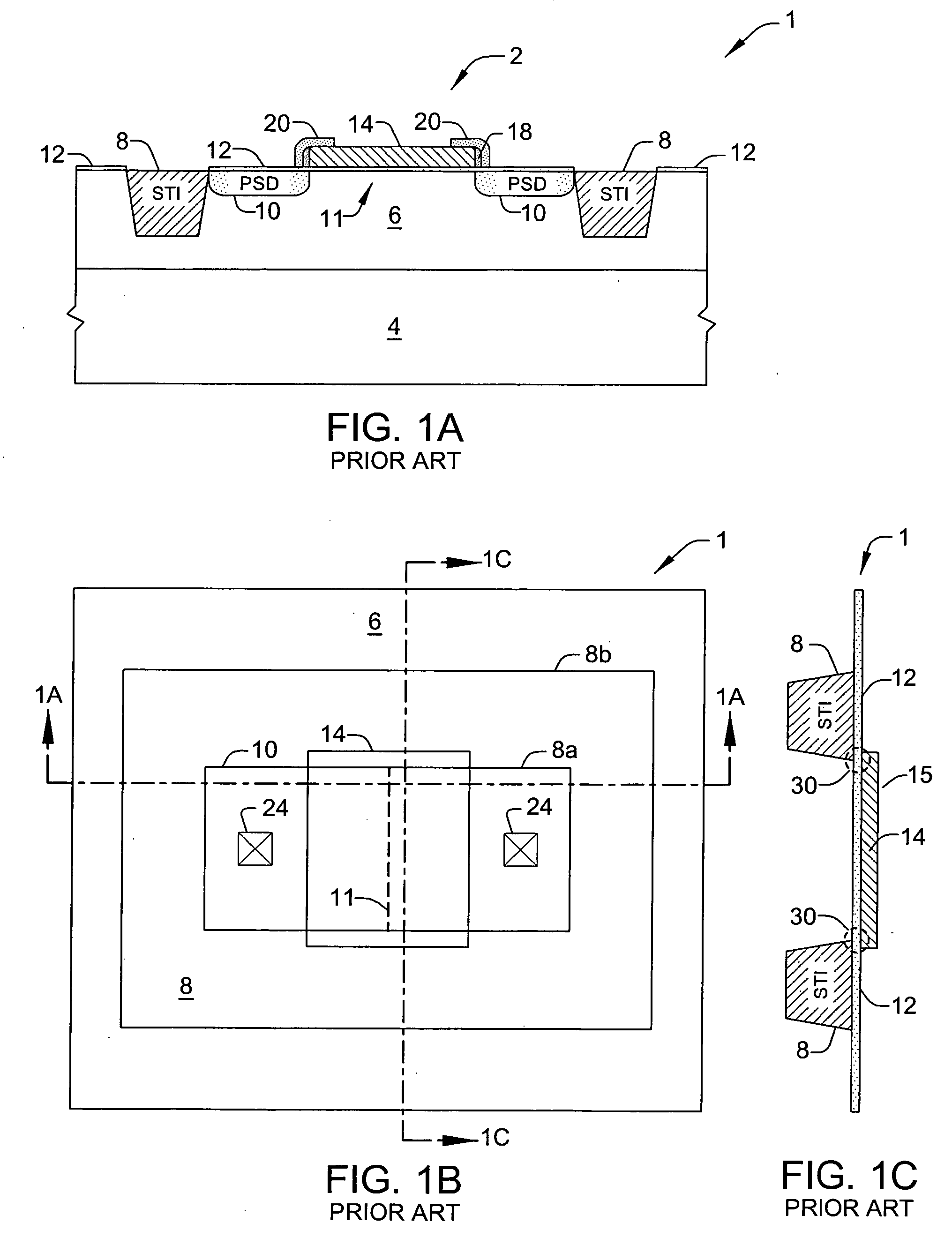
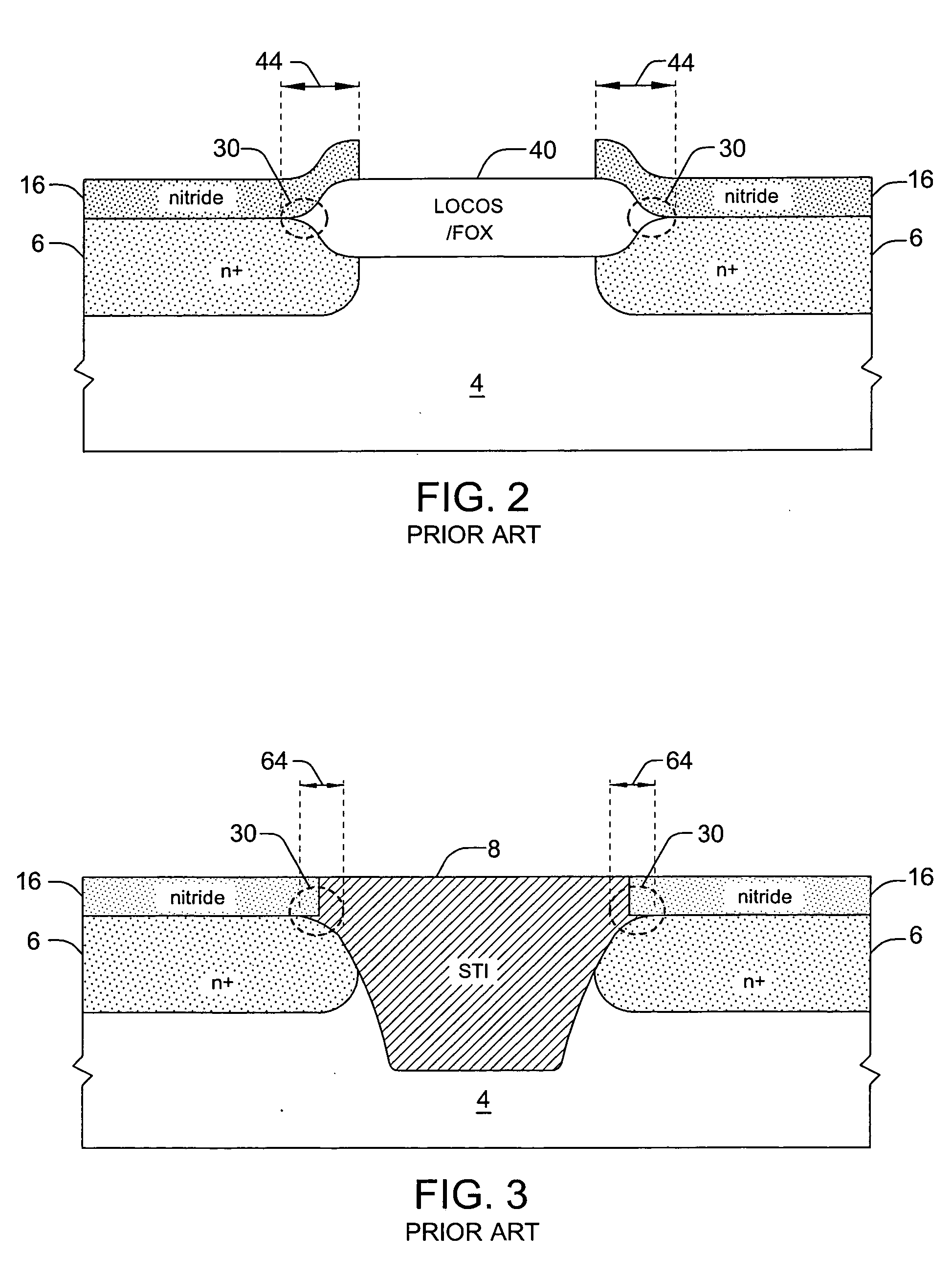
[0026] Conventional memory devices use an isolation barrier (e.g., an STI or LOCOS isolation structure) to isolate various elements of a semiconductor device and to define the boundaries of certain active regions in the substrate. Conventionally, however, the interface between these isolation structures and the active regions tend to produce birds-beak type regions that cause a non-uniform local thinning in the subsequent growth of a gate oxide layer. As a result, memory cells may experience a charg...
PUM
 Abstract
Description
Claims
Application Information