Element mapping unit, scanning transmission electron microscope, and element mapping method

a scanning transmission electron microscope and element mapping technology, applied in material analysis using wave/particle radiation, instruments, nuclear engineering, etc., can solve the problems of difficult to acquire element distribution images in real time, large amount of time, and difficult to obtain two-dimensional images, so as to improve the operability of an analyzer concerning eels, less effect of chip noise, and high eels spectrum energy stability

Inactive Publication Date: 2006-01-19
HITACHI LTD
View PDF10 Cites 33 Cited by
  • Summary
  • Abstract
  • Description
  • Claims
  • Application Information

AI Technical Summary

Benefits of technology

[0017] Another object of the present invention is to improve the operability of an analyzer concerning EELS and/or STEM.
[0018] Another object of the present invention is to provide an apparatus with high EELS spectrum energy stability.
[0019] Another object of the present invention is to provide an energy filter for an element mapping

Problems solved by technology

Acquiring a two-dimensional image, however, takes a vast amount of time and therefore, acquiring an element distribution image in real time is difficult.
With this method, however, measurement data results in a vast amount and an element distribution image cannot be acquired in real time.
When

Method used


Image

  • Element mapping unit, scanning transmission electron microscope, and element mapping method
  • Element mapping unit, scanning transmission electron microscope, and element mapping method
  • Element mapping unit, scanning transmission electron microscope, and element mapping method

Examples


first embodiment

The First Embodiment

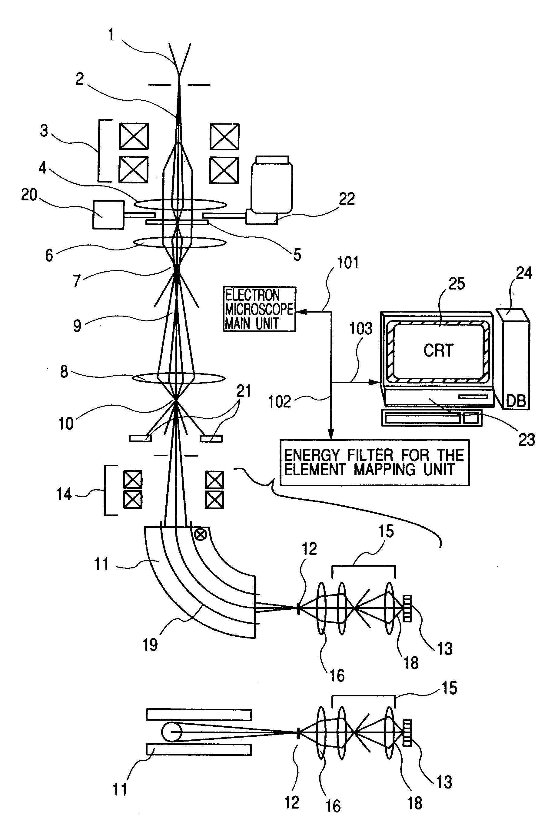
[0052]FIG. 1 is a schematic block diagram showing the main portion of a scanning transmission electron microscope (hereinafter, sometimes called the electron microscope) equipped with an energy filter for an element mapping unit according to an embodiment of the present invention. FIG. 1 (a) is a front view and FIG. 1 (b) is a view (plan view) of FIG. 1 (a) from an electron beam source 1. In this figure, the electron microscope body includes the components from an electron source 1 up to a Z contrast detector 21. The electron microscope contains structures, not shown, for controlling the electron beam scanning and others so as to function as an electron microscope. The portion from a sextuple electromagnetic lens 14 up to an electron beam detector 13 is shown as the energy filter for an element mapping unit. Signals to and from a computation unit 23 are transmitted via a signal line 103. Connected to the computation unit 23 are an input device such as keyboard, d...

second embodiment

[0090] The second embodiment of the present invention is explained hereunder. This embodiment covers an example of an element mapping unit wherein an element to be observed can be changed to another in the course of the observation so as to acquire a distribution image of multiple elements and observation position can be varied or observation magnification can be varied while observing an element distribution image.

[0091]FIG. 6 shows an energy filter and control unit 50. For the energy filter in this embodiment, the electron beam detector 13 is installed at the position where the energy scattering plane 12 of the energy filter in the first embodiment is located, and the focus-adjusting electromagnetic lens 16 is provided upstream the electron spectrometer 11 and the magnifying lens 15 down stream the electron spectrometer 11.

[0092] In this embodiment, a scanning transmission electron microscope (STEM) explained in the first embodiment is employed (Refer to FIG. 1). A 1024-channel ...


PUM


Abstract

There is provided an element mapping unit, scanning transmission electron microscope, and element mapping method that enable to acquire an element mapping image very easily. On the scanning transmission electron microscope, the electron beam transmitted through an object to be analyzed enters into the element mapping unit. The electron beam is analyzed of its energy into spectrum by an electron spectrometer and an electron energy loss spectrum is acquired. Because the acceleration voltage data for each element and window data for 2-window method, 3-window method or contrast tuning method are already stored in a database and accordingly the spectrum measurement is carried out immediately even when an element to be analyzed is changed to another, the operator can confirm a two-dimensional element distribution map immediately. Besides, because every electron beam that enters into an energy filter passes through the object point, aberration strain in the electron spectrometer can be minimized and higher energy stability can be achieved. As a result, drift of the electron energy loss spectrum acquired by analyzing the electron beam into spectrum can be minimized and element distribution with higher accuracy can be acquired.

Description

TECHNICAL FIELD [0001] The present invention relates to an element mapping unit, scanning transmission electron microscope, and element mapping method. BACKGROUND ART [0002] As semiconductor element or magnetic head element has become smaller and more compact, the element is now structured by laminated thin films of several NMs (nanometers) within a micro region of submicrons. Since the performance of the semiconductor element or magnetic head element depends upon the structure, element distribution and crystal structure of the micro region, analysis of the micro region is very important. [0003] For observation of the micro region, there are available a scanning electron microscope (SEM), transmission electron microscope (TEM), and scanning transmission electron microscope (STEM). TEM is an apparatus in which electron beams are irradiated onto a specimen nearly in parallel and the transmitted electron beams are magnified by a lens. STEM is an apparatus in which electron beams are co...

Claims


Application Information

Patent Timeline
IPC IPC(8): G21K7/00G01N23/00H01J37/256
CPCH01J37/256
Inventor KAJI, KAZUTOSHIUEDA, KAZUHIROKIMOTO, KOJIAOYAMA, TAKASHITAYA, SHUNROKUISAKOZAWA, SHIGETO
Owner HITACHI LTD
Why Eureka
Try Eureka