Method and apparatus for sample formation and microanalysis in a vacuum chamber

a vacuum chamber and sample technology, applied in semiconductor/solid-state device testing/measurement, instruments, therapy, etc., can solve the problems of brittle thin samples extracted from wafers, affecting reducing the economic impact of defect analysis on the overall cost of manufacturing process, so as to achieve the effect of reducing the economic impact of defect analysis and facilitating automation

Active Publication Date: 2006-01-19
APPL MATERIALS ISRAEL LTD
View PDF12 Cites 70 Cited by
  • Summary
  • Abstract
  • Description
  • Claims
  • Application Information

AI Technical Summary

Benefits of technology

[0100] In a particular embodiment, the alternate ion beam milling and electron microscopy imaging are performed in situ when the sample is mounted on a sample support. It is noted that for some embodiments, this allows for the mounting of thicker and more stable samples than would otherwise be used.
[0101] Although certain embodiments of the invention do not preclude the precleaving of an object or semiconductor wafer before sample formation, the techniques of the present invention do not require the wafer to be precleaved before extracting the samples, and do not require me

Problems solved by technology

The conventional methods for studying structures by an optical microscope cannot be used to study features in a modem electronic structure due to the unacceptable resolution of an optical microscope.
Although TEM techniques can provide a higher resolution image and a more detailed description of the internal structure of a than is available using SEM techniques, they a

Method used


Image

  • Method and apparatus for sample formation and microanalysis in a vacuum chamber
  • Method and apparatus for sample formation and microanalysis in a vacuum chamber
  • Method and apparatus for sample formation and microanalysis in a vacuum chamber

Examples


Embodiment Construction

[0129] It should be understood that the class of embodiments described herein provides only a few examples of the many advantageous uses of the innovative teachings herein. In general, statements made in the specification of the present application do not necessarily delimit any of the various claimed inventions. Moreover, some statements may apply to some inventive features but not to others.

[0130] In accordance with many embodiments of the present invention, a disclosed method for sample formation begins with cutting of a portion of an object. In one specific embodiment, the object is a semiconductor wafer, though in other embodiments, exemplary objects include a biological material, a micromechanical device, a thin film, etc.

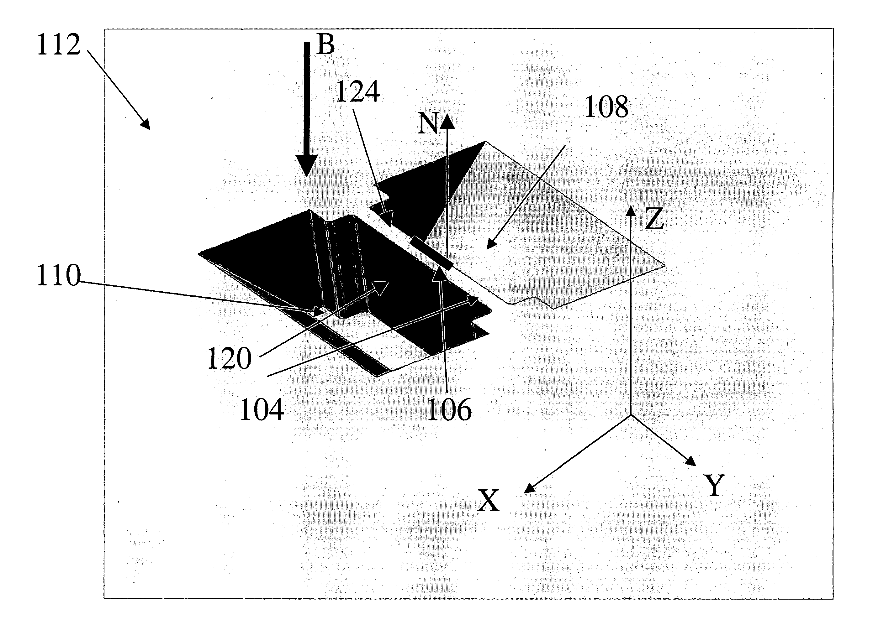
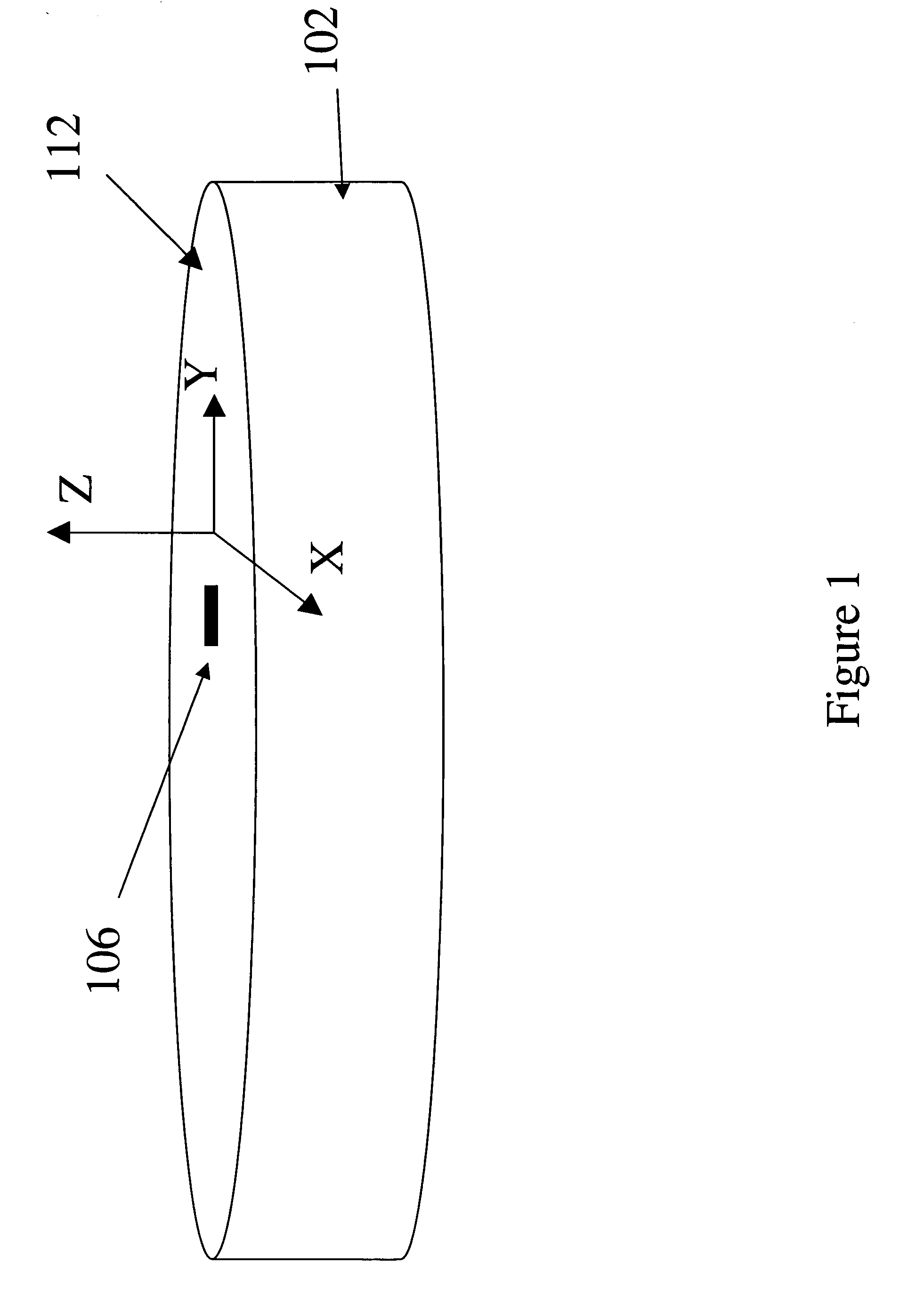
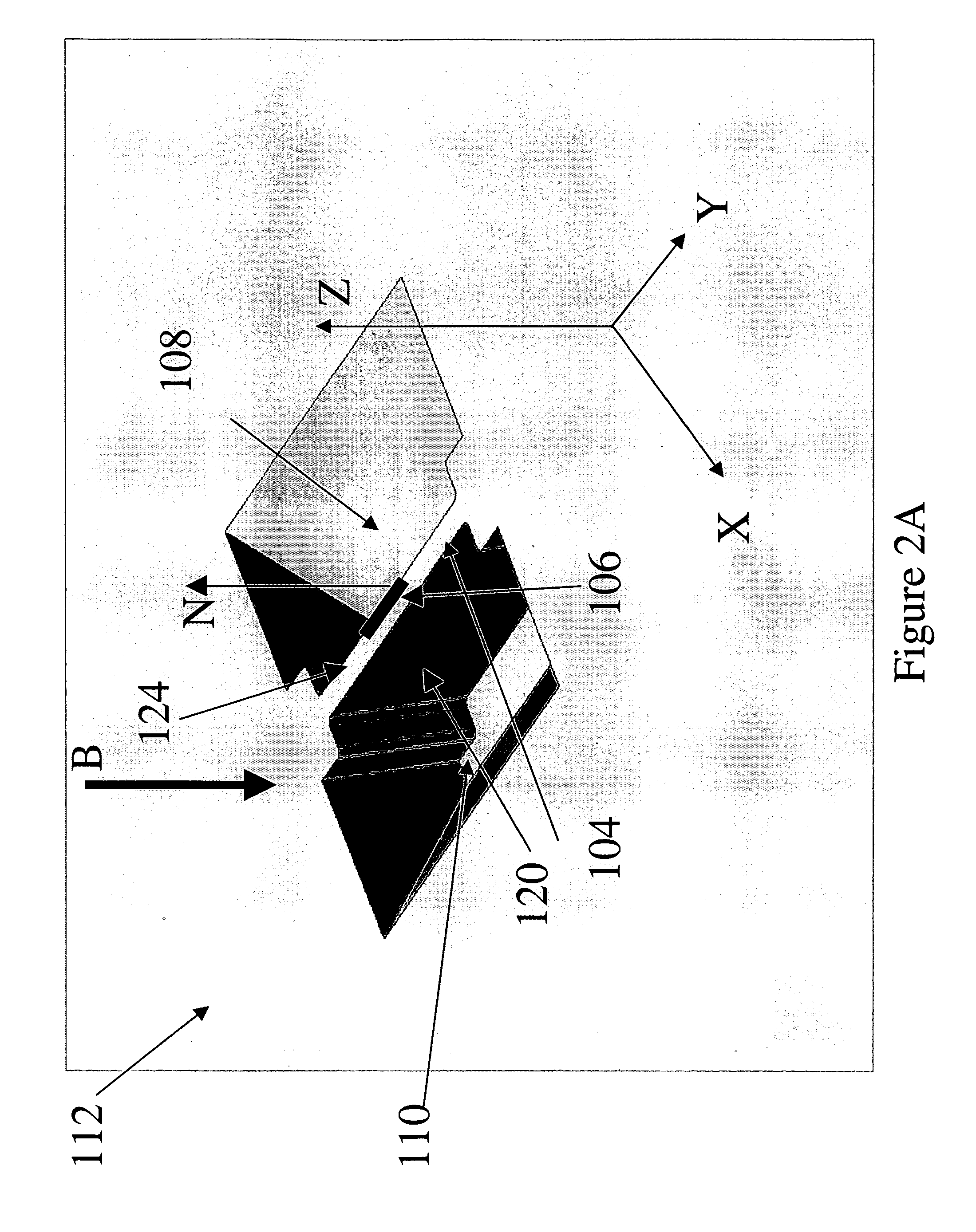
[0131]FIG. 1 provides an exemplary illustration of an object 102 from which a portion is to be extracted near a target location 106, the object 102 including an upper or outer surface 112. In FIG. 1, the object 102 depicted is of cylindrical shape, though t...


PUM


Abstract

Methods and apparatus are disclosed for forming a sample of an object, extracting the sample from the object, and subjecting this sample to microanalysis including surface analysis and electron transparency analysis in a vacuum chamber. In some embodiments, a method is provided for imaging an object cross section surface of an extracted sample. Optionally, the sample is iteratively thinned and imaged within the vacuum chamber. In some embodiments, the sample is situated on a sample support including an optional aperture. Optionally, the sample is situated on a surface of the sample support such that the object cross section surface is substantially parallel to the surface of the sample support. Once mounted on the sample support, the sample is either subjected to microanalysis in the vacuum chamber, or loaded onto a loading station. In some embodiments, the sample is imaged with an electron beam substantially normally incident to the object cross section surface.

Description

CROSS-REFERENCE TO RELATED APPLICATIONS [0001] This application claims priority to U.S. Provisional Application Ser. No. 60 / 588272, filed Jul. 14, 2004, which is incorporated herein by reference in its entirety.FIELD OF THE INVENTION [0002] The present invention relates generally to semiconductor device monitoring, and specifically to the preparation and imaging of thin samples for testing internal structure of fabricated devices. BACKGROUND OF THE INVENTION [0003] In the study of electronic materials and processes for fabricating such materials into an electronic structure, a specimen of the electronic structure is frequently used for microscopic examination for purposes of failure analysis and device validation. For instance, a specimen of an electronic structure such as a silicon wafer is frequently analyzed in scanning electron microscope (SEM) and transmission electron microscope (TEM) to study a specific characteristic feature in the wafer. Such characteristic feature may incl...

Claims


Application Information

Patent Timeline
IPC IPC(8): G21K5/10
CPCG01N1/32H01J37/185H01J37/20H01J37/28H01J37/3056H01J2237/31749H01J2237/20292H01J2237/204H01J2237/208H01J2237/31745H01J2237/20278H01L22/00
Inventor KIDRON, EITANSHEMESH, DROR
Owner APPL MATERIALS ISRAEL LTD
Why Eureka
Try Eureka