

Optical dna sensor, dna reading apparatus, identification method of dna and manufacturing method of optical dna sensor
- Summary
- Abstract
- Description
- Claims
- Application Information
AI Technical Summary
Benefits of technology
Problems solved by technology
Method used
Image

Examples
first embodiment
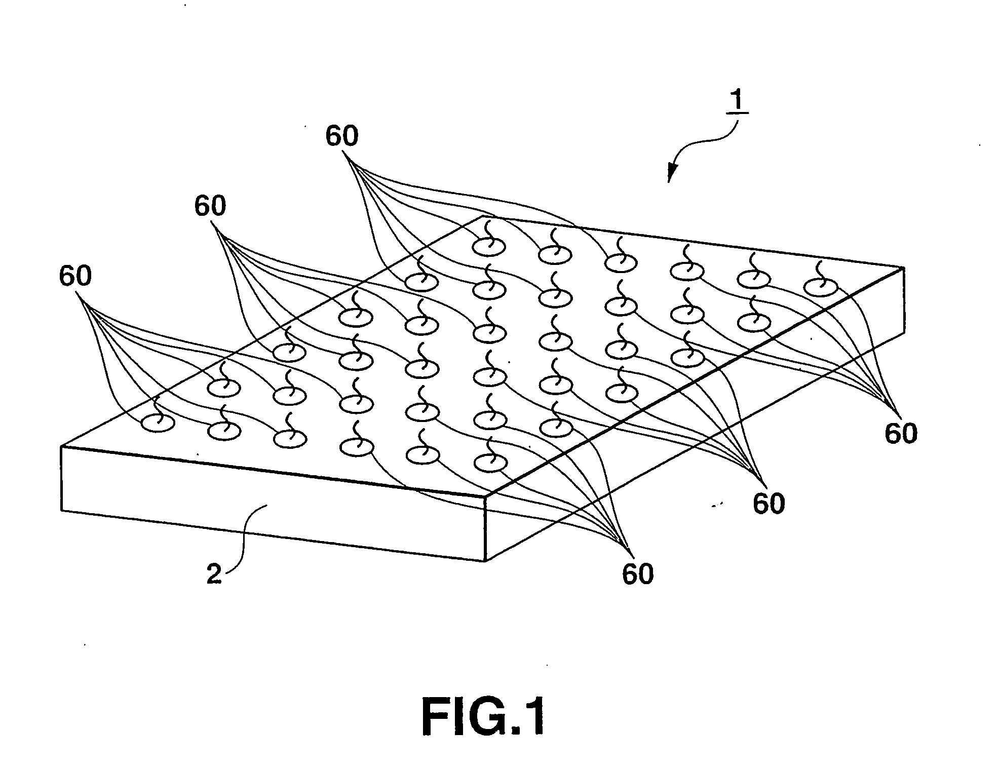
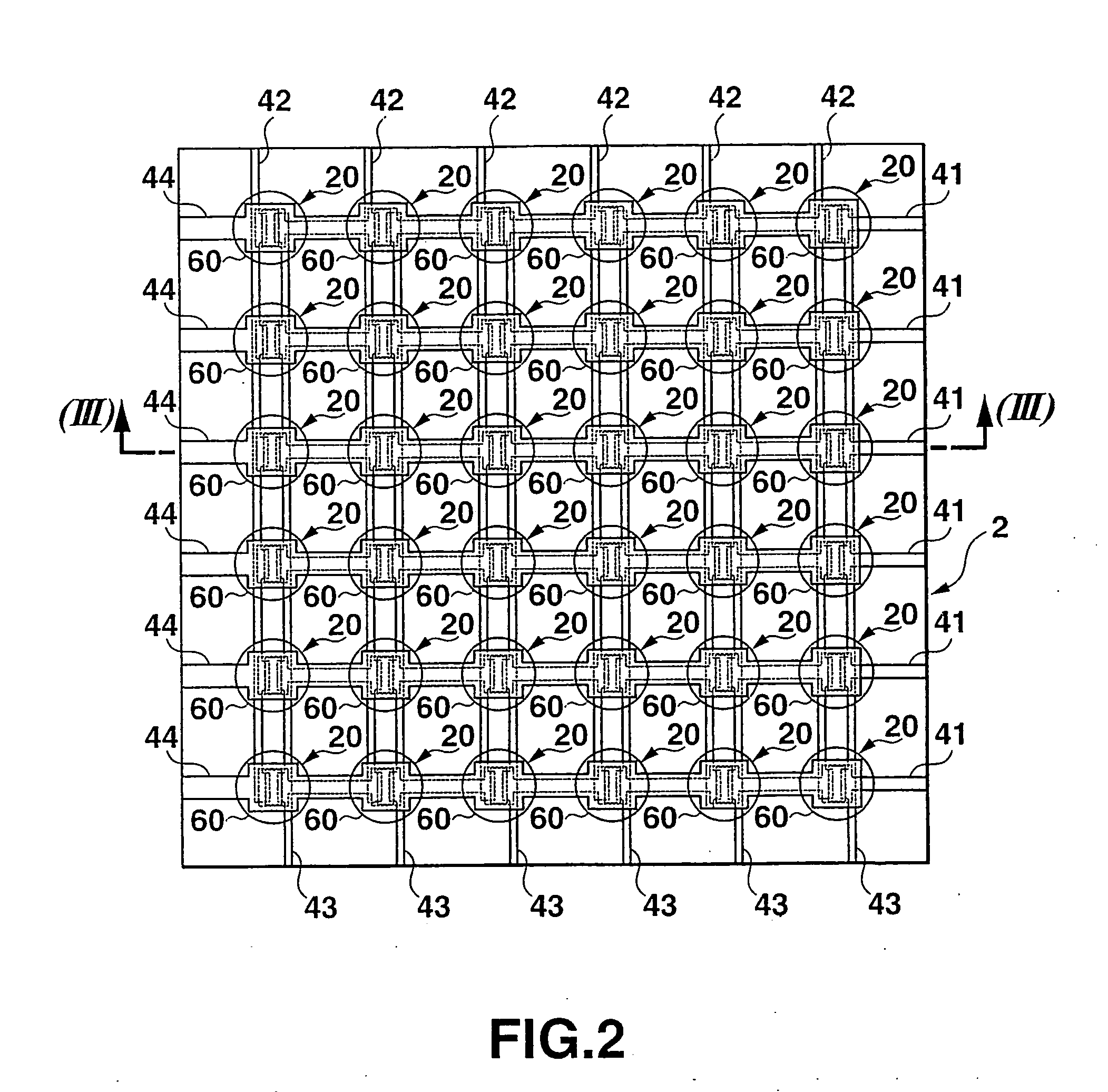
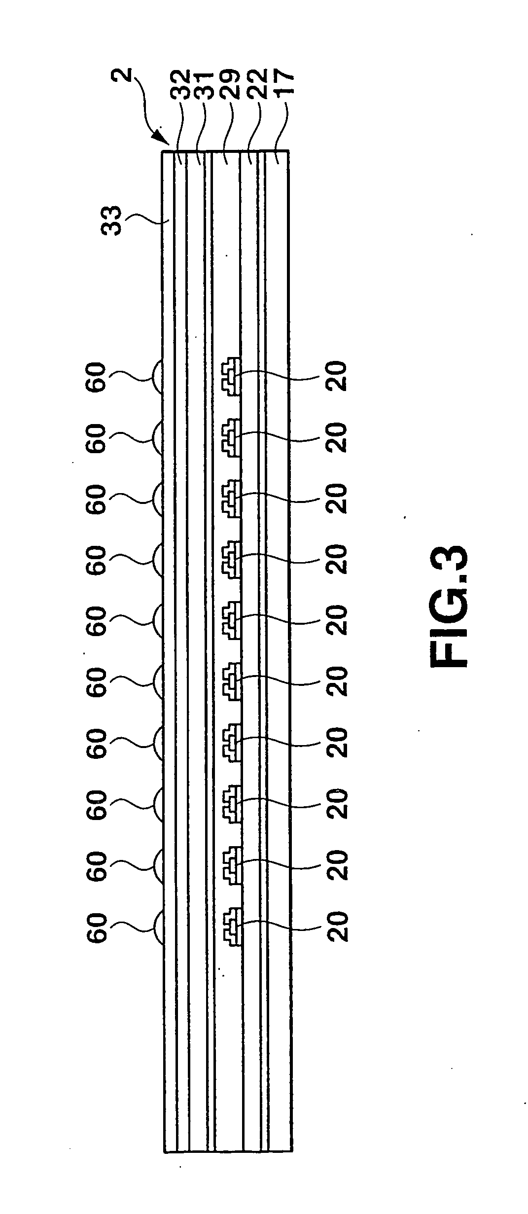
[0048]FIG. 1 is an oblique perspective view showing an optical DNA sensor to which the present invention is applied, FIG. 2 is a plan view of the optical DNA sensor, and FIG. 3 is a cross-section of the sensor when it is cut along a broken line (III)-(III) in FIG. 2 and observed to a direction indicated by arrows.
[0049] An optical DNA sensor 1 includes a solid imaging device 2 and spots 60, 60, . . . collocated and fixed on a surface of the solid imaging device 2, and in which each of the spots 60 is configured to correspond to each of pixels of the solid imaging device 2.
[0050] First, the solid imaging device will be explained below. The solid imaging device 2 includes a transparent substrate 17 of a substantially flat plate shape, photo-sensor elements (hereinafter referred to as sensors) 20, 20, . . . including a plurality of double gate type field-effect transistors those which are arranged in a matrix fashion consisting of n lines and m rows, (wherein both n and m are a posit...
second embodiment
[0108]FIG. 9 is a plan view showing an optical DNA sensor according to the second embodiment, and FIG. 10 is a cross-section of the optical DNA sensor when it is cut along a broken line (X)-(X) indicated in FIG. 9 and observed to a direction indicated by arrows.
[0109] In the optical DNA sensor 1 according to the first embodiment, one sensor 20 corresponds to one spot 60. Unlike that, in the optical DNA sensor 100 according to the second embodiment, sensors 20 are fixed on the surface of a solid imaging device such that four sensors 20 correspond to one spot 60. Specifically, in the optical DNA sensor according to the second embodiment, four adjacent sensors 20 in the vertical and horizontal directions form a set, and one spot corresponds to the set. When observing in a plan view, four sensors 20 are superimposed on one spot 60. Note that the neighbor spots 60 are distanced to each other.
[0110] The other components of the optical DNA sensor of this embodiment are equivalent to thos...
third embodiment
[0114] As shown in FIG. 11, the optical DNA sensor according to the third embodiment is structured by additionally including an excited light absorbing layer 34 to the optical DNA sensor according to either of the above-described embodiments. FIG. 11 is a cross-section of the optical DNA sensor of the third embodiment which is similar to the sensor of the first embodiment shown in FIG. 3.
[0115] The optical DNA sensor 1 of this embodiment includes a solid imaging device 2, an excited light absorbing layer 34 formed on the surface of the solid imaging device and made from a titanium oxide layer with a fixed thickness, and spots 60, 60, . . . arrayed and fixed on the excited light absorbing layer 34, wherein each of the spots 60 corresponds to each of pixels of the solid imaging device.
[0116] The solid imaging device 2 includes a transparent substrate 17 in a substantially flat plate shape and sensors 20, 20, . . . each having a plurality of double gate type field-effect transistors ...
PUM
| Property | Measurement | Unit |
|---|---|---|
| Thickness | aaaaa | aaaaa |
| Electrical conductor | aaaaa | aaaaa |
| Transparency | aaaaa | aaaaa |
Abstract
Description
Claims
Application Information