Method of forming titanium nitride layer and method of fabricating capacitor using the same

a technology of titanium nitride and fabrication method, which is applied in the direction of solid-state devices, coatings, chemical vapor deposition coatings, etc., can solve the problems of deterioration of signal-to-noise ratio (s/n ratio), soft error due to alpha () particles, and deterioration of interface characteristics between the dielectric layer and the electrode of the storage capacitor

Active Publication Date: 2006-01-19
SAMSUNG ELECTRONICS CO LTD
View PDF23 Cites 33 Cited by
  • Summary
  • Abstract
  • Description
  • Claims
  • Application Information

AI Technical Summary

Benefits of technology

[0021] Embodiments of the invention provide methods of forming a titanium nitride layer that suppress the generation of hafnium

Problems solved by technology

When the capacitance of the storage capacitor is decreased, the signal-to-noise ratio (S/N ratio) deteriorates, and a soft error due to an alpha (α) particle may occur.
When a high dielectric material such as Ta2O5, Al2O3, or HfO2 is employed for the dielectric layer of the storage capacitor, even though the dielectric constant is increased, the interface characteristics between the dielectric layer and the polycrystalline silicon used as an electrode of the storage capacitor may deteriorate.
F

Method used


Image

  • Method of forming titanium nitride layer and method of fabricating capacitor using the same
  • Method of forming titanium nitride layer and method of fabricating capacitor using the same
  • Method of forming titanium nitride layer and method of fabricating capacitor using the same

Examples


Embodiment Construction

[0025] The teachings of the invention will now be described more fully hereinafter with reference to the accompanying drawings, in which preferred embodiments of the invention are shown. This invention may, however, be embodied in different forms and should not be construed as limited to the embodiments set forth herein. Like numbers refer to like elements throughout.

[0026]FIGS. 1a through 1k are sectional diagrams illustrating a method of fabricating a capacitor of a semiconductor device according to some embodiments of the invention. For purposes of illustration, the semiconductor device will be assumed to be a DRAM device, although other types of semiconductor devices could be fabricated.

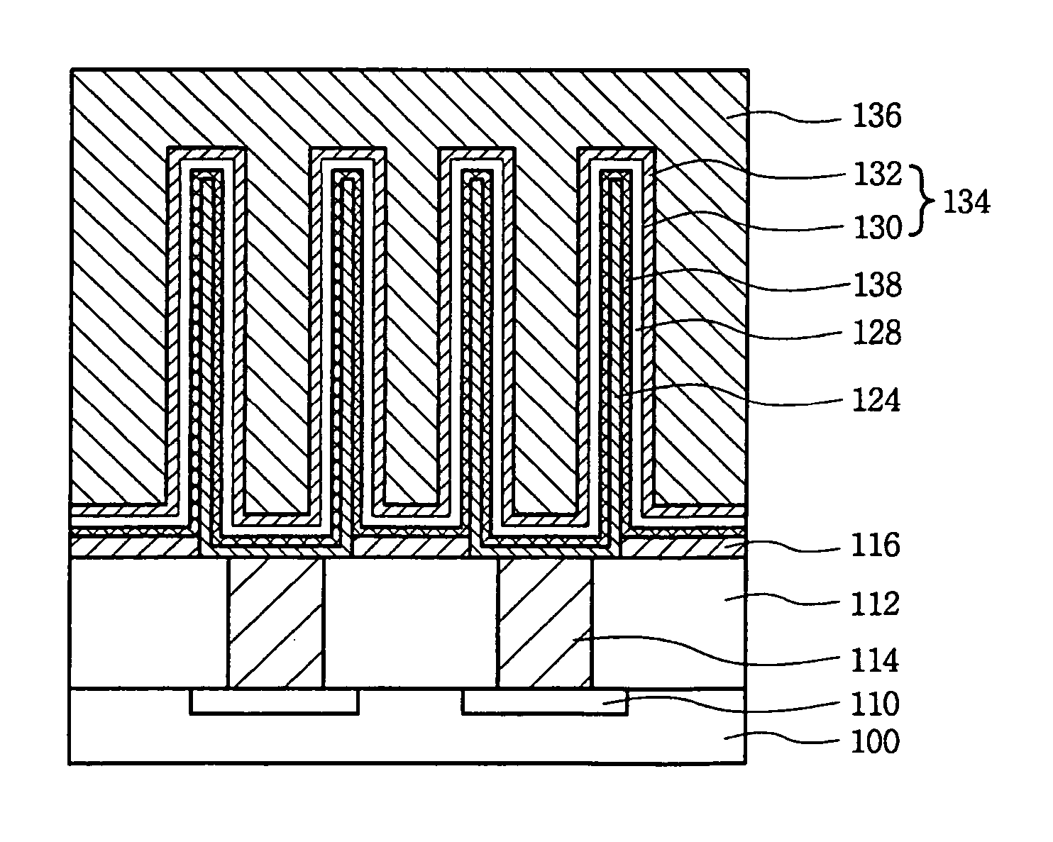
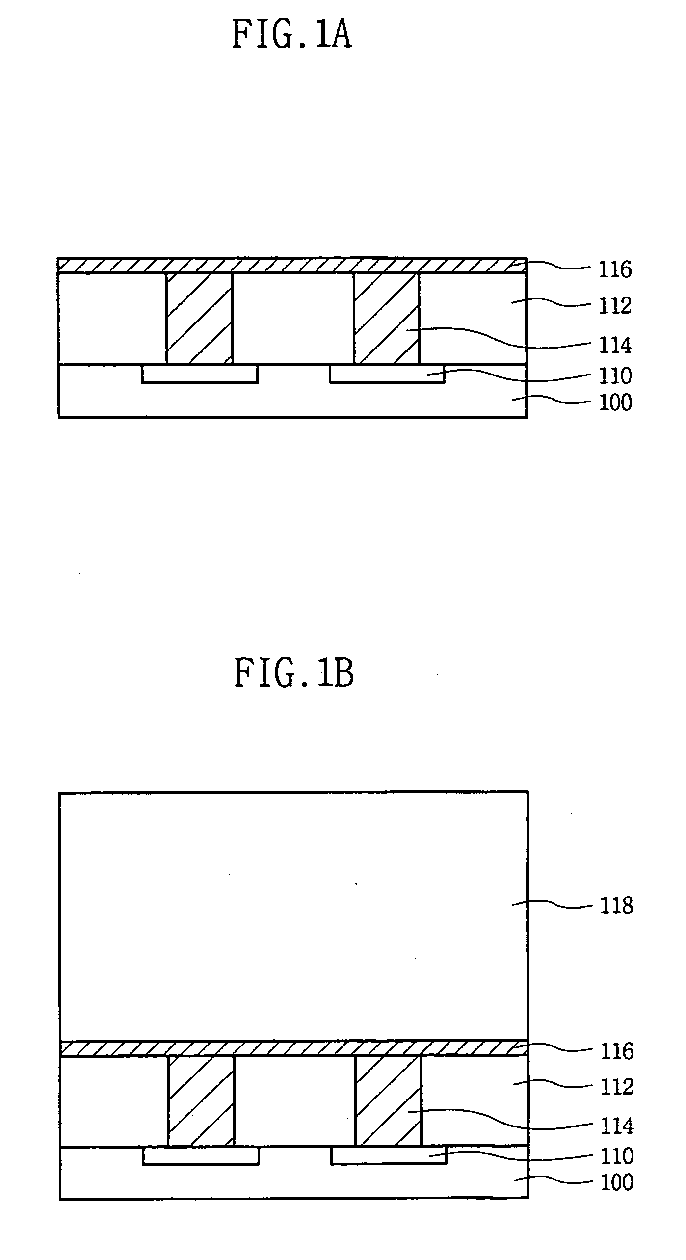
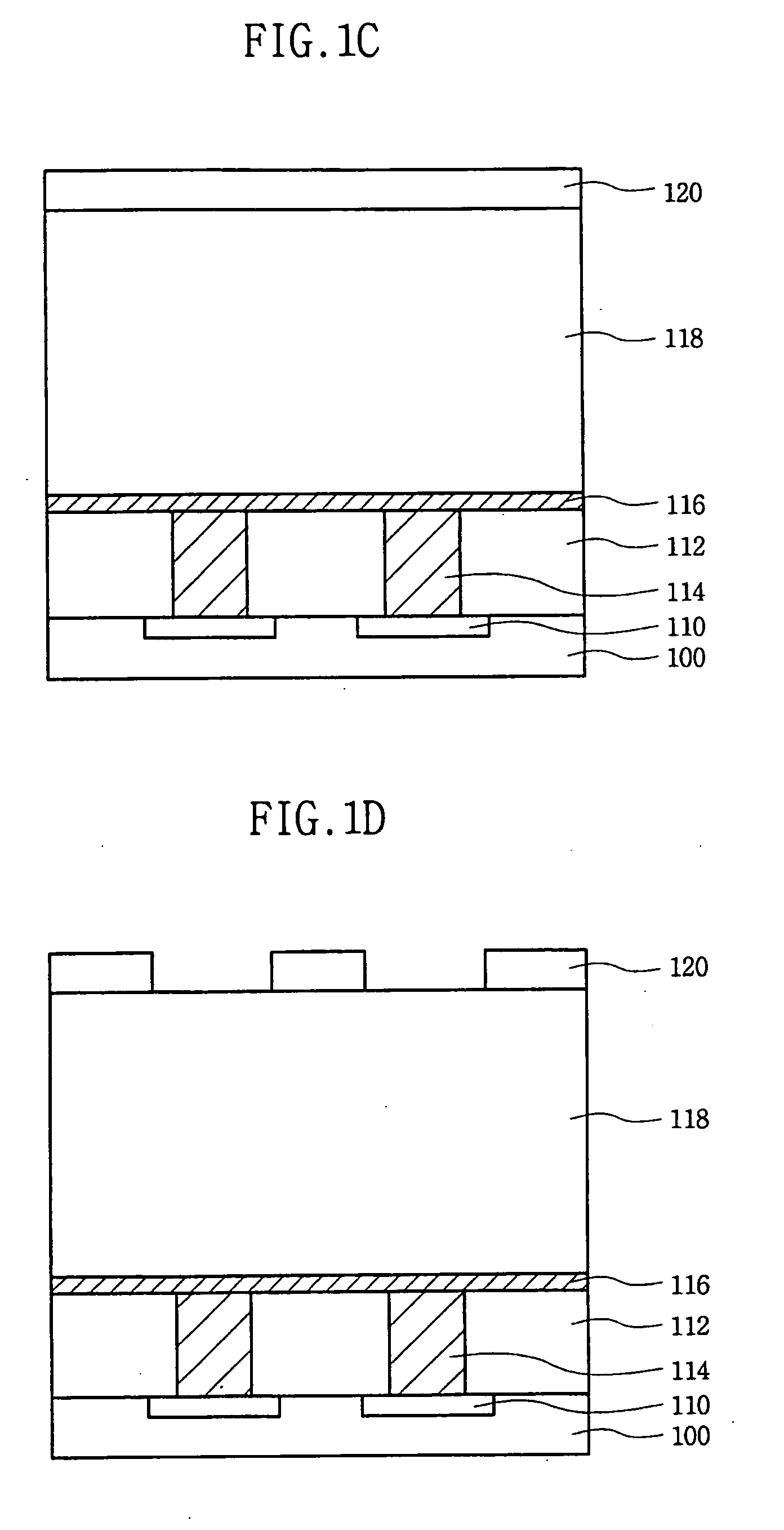
[0027] Referring to FIG. 1A, an etch stop layer 116 is formed on a semiconductor substrate 100 having an interlayer insulating layer 112 and a conductive structure 114. The etch stop layer 116 may be composed of silicon nitride. The conductive structure 114 may be a contact plug that is electri...


PUM

PropertyMeasurementUnit
Temperatureaaaaaaaaaa
Pressureaaaaaaaaaa

Abstract

A method of fabricating a storage capacitor includes depositing a first titanium nitride layer on a dielectric layer using a chemical vapor deposition technique or an atomic layer deposition technique performed at a first temperature with reactant gases of titanium chloride (TiCl4) gas and ammonia (NH3) gas at a predetermined flow ratio and depositing a second titanium nitride layer on the first titanium nitride layer using a chemical vapor deposition process performed at a second temperature that is greater than the first temperature with reactant gases of titanium chloride (TiCl4) gas and ammonia (NH3) gas.

Description

CROSS REFERENCE TO RELATED APPLICATIONS [0001] This application claims priority from Korean Patent Application No. 10-2004-0055004, filed 15 Jul. 2004, the content of which is hereby incorporated by reference in its entirety, for all purposes. BACKGROUND [0002] 1. Technical Field [0003] This disclosure is generally related to semiconductor devices, and, more particularly, to methods of forming a metal electrode from a titanium nitride layer to prevent a leakage current, and to methods of fabricating a storage capacitor having the metal electrode. [0004] 2. Description of the Related Art [0005] It is widely known that a memory cell of a semiconductor memory device, such as a dynamic random access memory (DRAM), includes one transistor and one storage capacitor. When the size of the memory cell is reduced in response to an increased degree of integration on the DRAM, the size of the transistor is also reduced as well as the area of the semiconductor substrate occupied by the storage c...

Claims


Application Information

Patent Timeline
IPC IPC(8): H01L21/20H01L21/44
CPCC23C16/34C23C16/45529H01L28/91H01L27/10852H01L28/75H01L27/10817H10B12/318H10B12/033H01L21/205H10B99/00
Inventor KIM, RAK-HWANLIM, HYUN-SEOKCHO, YOUNG-JOOPARK, IN-SUNLEE, HYEON-DEOKLEE, HYUN-SUK
Owner SAMSUNG ELECTRONICS CO LTD
Why Eureka
Try Eureka