Low-temperature plasma-enhanced chemical vapor deposition of silicon-nitrogen-containing films

a technology of chemical vapor deposition and silicon nitrogen, which is applied in the field of substrate processing, can solve the problems of high deposition temperature and incompatible with advanced device processing requiring a low thermal budget, and achieve the effect of improving the chemical vapor deposition efficiency

Inactive Publication Date: 2006-01-19
TOKYO ELECTRON LTD
View PDF4 Cites 106 Cited by
  • Summary
  • Abstract
  • Description
  • Claims
  • Application Information

AI Technical Summary

Benefits of technology

[0007] A system and method are provided for low-temperature plasma-enhanced deposition of silicon-nitrogen-containing films on a substrate. To this end, the method includes providing a substrate in a process chamber, exciting a reactant gas in a remote plasma source, thereafter mixing the excited reactant gas with a silazane precursor gas, and depositing a silicon-nitrogen-containing film on the substrate from the excited gas mixture in a chemical vapor deposition process.
[0008] In one embodiment of the invention, a method is provided for low-temperature plasma-enhanced deposition of a SiCNH film on a substrate. The method includes providing a substrate in a process chamber, exciting a nitrogen-containing reactant gas in a remote plasma source, thereafter mixing the excited reactant gas with a silazane precursor

Problems solved by technology

In addition, plasma excitation may activate film-forming chemical reactions that are not energetically or kinetically favored in thermal CVD.
However, the explosive behavior of SiH4 and corrosive behavior of SiH2Cl2 requires strict control ov

Method used


Image

  • Low-temperature plasma-enhanced chemical vapor deposition of silicon-nitrogen-containing films
  • Low-temperature plasma-enhanced chemical vapor deposition of silicon-nitrogen-containing films
  • Low-temperature plasma-enhanced chemical vapor deposition of silicon-nitrogen-containing films

Examples


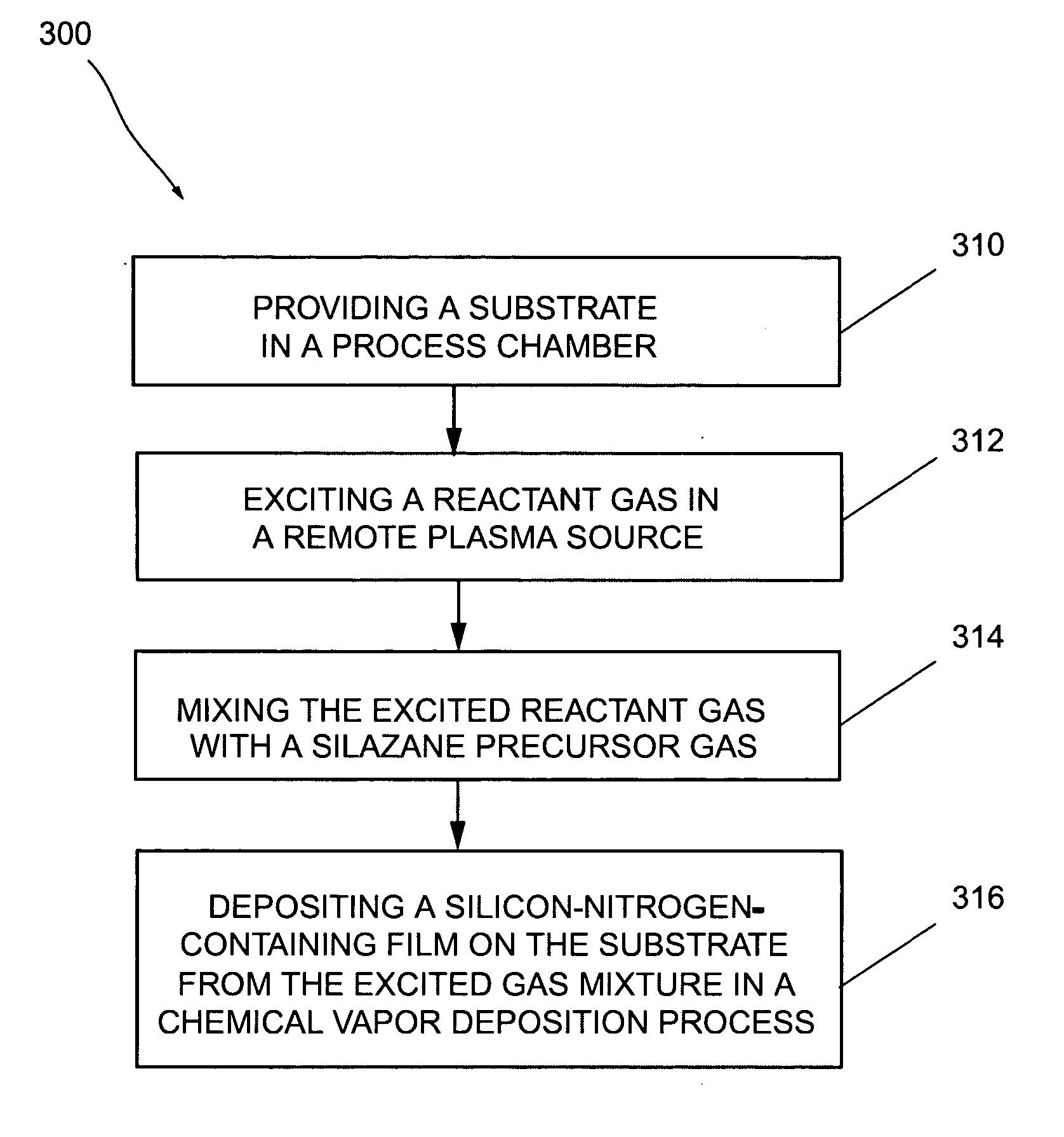
Embodiment Construction

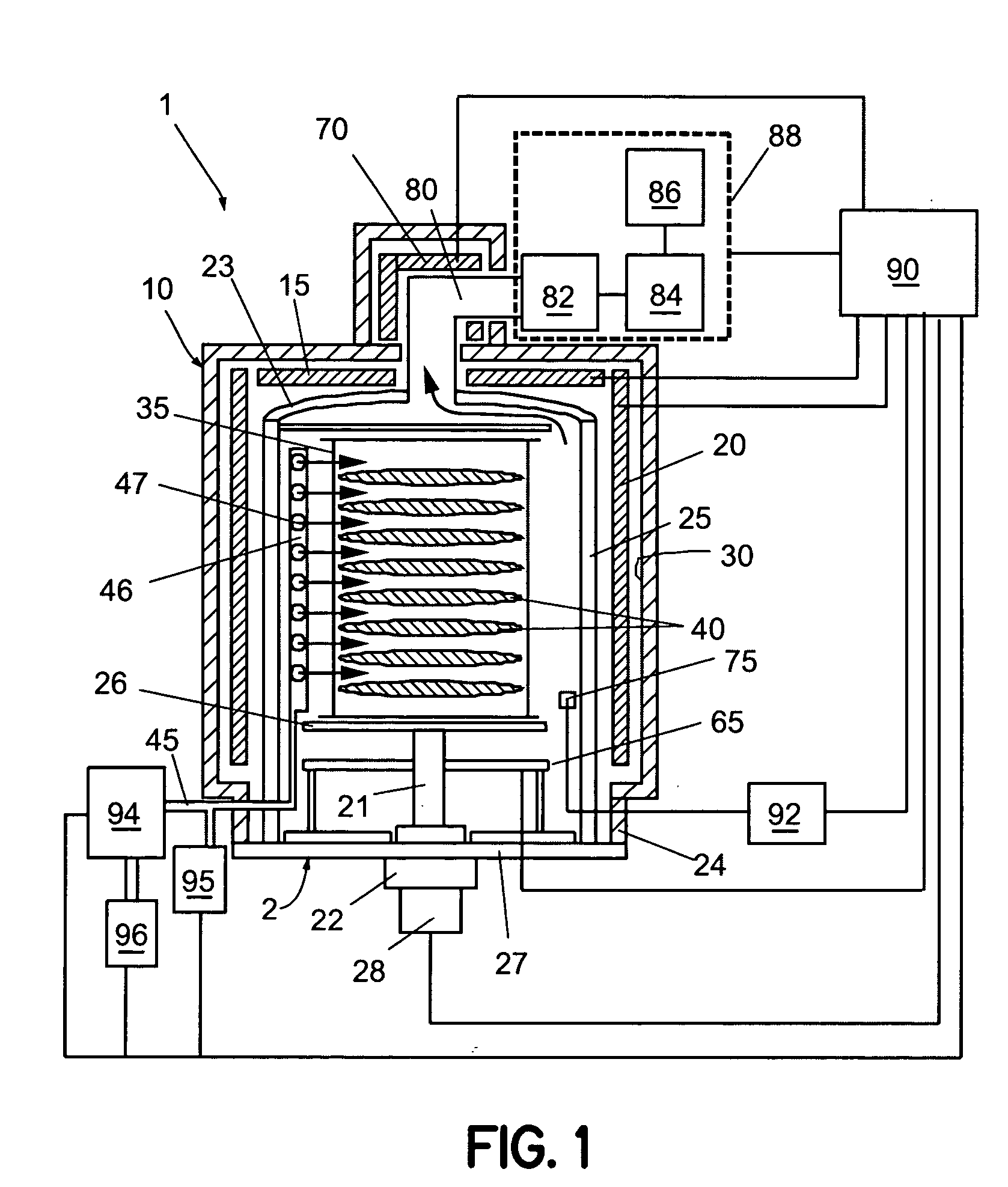
[0014]FIG. 1 shows a simplified block diagram of a batch-type processing system for low-temperature plasma-enhanced deposition of a silicon-nitrogen-containing film on a substrate according to an embodiment of the invention. The batch-type processing system 1 contains a process chamber 10 and a process tube 25 therein that has an upper end 23 connected to a exhaust pipe 80, and a lower end 24 hermetically joined to a lid 27 of cylindrical manifold 2. The exhaust pipe 80 discharges gases from the process tube 25 to a vacuum pumping system 88 to maintain a pre-determined reduced pressure in the processing system 1. A substrate holder 35 for holding a plurality of substrates (wafers) 40 in a tier-like manner (in respective horizontal planes at vertical intervals) is placed in the process tube 25. The substrate holder 35 resides on a turntable 26 that is mounted on a rotating shaft 21 penetrating the lid 27 and driven by a motor 28. The turntable 26 can be rotated during processing to i...


PUM

PropertyMeasurementUnit
Temperatureaaaaaaaaaa
Pressureaaaaaaaaaa

Abstract

A method for low-temperature plasma-enhanced chemical vapor deposition of a silicon-nitrogen-containing film on a substrate. The method includes providing a substrate in a process chamber, exciting a reactant gas in a remote plasma source, thereafter mixing the excited reactant gas with a silazane precursor gas, and depositing a silicon-nitrogen-containing film on the substrate from the excited gas mixture in a chemical vapor deposition process. In one embodiment of the invention, the reactant gas can contain a nitrogen-containing gas to deposit a SiCNH film. In another embodiment of the invention, the reactant gas can contain an oxygen-containing gas to deposit a SiCNOH film.

Description

FIELD OF THE INVENTION [0001] The present invention relates to substrate processing, and more particularly, to a method for low-temperature plasma-enhanced chemical vapor deposition of a silicon-nitrogen-containing film on a substrate. BACKGROUND OF THE INVENTION [0002] Silicon-containing films are used for a wide variety of applications in the semiconductor industry. Silicon-containing films include silicon films such as polycrystalline silicon (poly-Si) and epitaxial silicon, silicon germanium (SiGe), silicon germanium carbide (SiGeC), silicon carbide (SiC), silicon nitride (SiN), silicon carbonitride (SiCN), and silicon carboxide (SiCO). Various physical and / or chemical deposition techniques are routinely employed for silicon-containing film deposition, and often more than one technique may be used to deposit a particular film. The preferred deposition method is determined by considering the desired film properties, physical and / or chemical constraints imposed by the device being...

Claims


Application Information

Patent Timeline
IPC IPC(8): H01L21/31H01L21/469
CPCC23C16/30C23C16/345H01L21/3185H01L21/3125C23C16/452H01L21/02274H01L21/02115H01L21/0217H01L21/02222H01L21/02271H01L21/02126H01L21/02167
Inventor JOE, RAYMOND
Owner TOKYO ELECTRON LTD
Why Eureka
Try Eureka