Check patentability & draft patents in minutes with Patsnap Eureka AI!

Dry etching method

a technology of silicon nitride and etching method, which is applied in the direction of decorative arts, electrical equipment, cable/conductor manufacturing, etc., can solve the problems of reduced initial increased trenches of sti, and reduced thickness of silicon nitride mask, so as to facilitate the control of the cmp process and improve the process accuracy of the round profile. , the effect of improving the process accuracy

Inactive Publication Date: 2006-01-26
HITACHI HIGH-TECH CORP
View PDF3 Cites 8 Cited by
  • Summary
  • Abstract
  • Description
  • Claims
  • Application Information

AI Technical Summary

Benefits of technology

[0008] The object of the present invention is to provide a round profile processing to the edge portion of the silicon nitride film mask while maintaining the initial film thickness of the mask and to independently control the round profile of the mask edge portion, thereby improving the processing accuracy.
[0010] According to the present processing method, the etching process is performed with the resist mask remaining on the silicon nitride film, so the initial thickness of the silicon nitride film mask will not be reduced by etching. Since it is possible to ensure a determined amount of silicon nitride film mask used as the stopper film for a chemical-mechanical polishing (CMP) process, control of the CMP process is facilitated. Moreover, since the round profile of the mask edge portion can be controlled independently, the process accuracy of the round profile processing is improved, and thus the occurrence of a cavity during the embedding step can be suppressed.
[0011] In other words, according to the present invention, the edge portion of the silicon nitride film mask can be processed to have a round profile while maintaining the initial film thickness of the silicon nitride film, and the round profile of the silicon nitride film can be independently controlled via the step of cutting back the resist mask, so the process accuracy of the round profile can be improved.

Problems solved by technology

Along with the miniaturization and enhanced integration of the semiconductor devices, the aspect ratio of the trenches of the STI has become higher, by which a problem occurs in which cavities are formed in the insulating film during the embedding process according to the low-pressure high-density plasma CVD method due to the limitation of the embedding performance.
According further to the prior art method, the photoresist is removed prior to the process of forming the trench for STI, so the thickness of the film is reduced by the etching performed during the trench formation process, and a problem occurs in which the initial thickness of the silicon nitride mask is reduced.
Moreover, according to the prior art method, the round profile of the edge portion depends on the etching conditions for forming the trench of the STI, so it was difficult to control the profile.

Method used


Image

  • Dry etching method
  • Dry etching method
  • Dry etching method

Examples


Embodiment Construction

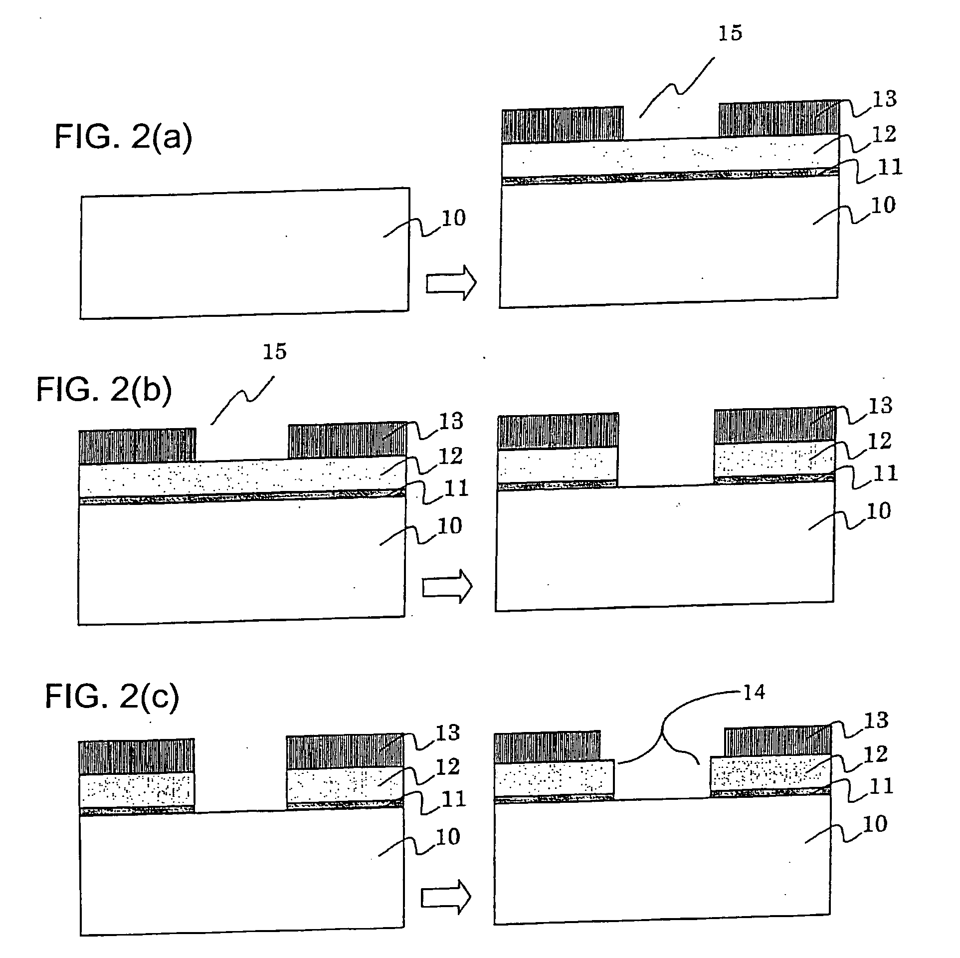
[0015] The plasma etching method according to the present invention will now be explained. FIG. 1 shows an etching apparatus used in the present invention. The present embodiment is an example in which a microwave plasma etching apparatus utilizing microwaves and magnetic field as plasma generating means is applied. Microwaves are generated by a magnetron 1, sent via a waveguide 2 and passed through a quartz plate 3 to be radiated into a vacuum vessel. A solenoid coil 4 is disposed around the vacuum vessel, and a magnetic field created via the coil and the radiated microwaves cause an electron cyclotron resonance (ECR). Thereby, a process gas is effectively turned into plasma 5 having high density. A process wafer 6 is held on an electrode via electrostatic chucking force, by applying a DC voltage to a wafer stage 8 from an electrostatic chucking power supply 7. Moreover, an RF power supply 9 is connected to the electrode for applying RF power (RF bias) to the electrode so as to pro...


PUM

PropertyMeasurementUnit
pressureaaaaaaaaaa
pressureaaaaaaaaaa
pressureaaaaaaaaaa

Abstract

The object of the invention is to provide a dry etching method for processing the edge portion of a hard mask to have a round profile. The present method for manufacturing a semiconductor device comprises (b) forming a silicon nitride film 12 mask using a patterned photoresist 13, (c) cutting back the photoresist 13 via dry etching, and (d) etching the exposed edge portion of the silicon nitride film mask 12, to thereby enable trench processing using a silicon nitride film mask 12 having a rounded edge portion.

Description

[0001] The present application is based on and claims priority of Japanese patent application No. 2004-217390 filed on Jul. 26, 2004 and No. 2004-225668 filed on Aug. 2, 2004, the entire contents of which are hereby incorporated by reference. FIELD OF THE INVENTION [0002] The present invention relates to a method for etching a semiconductor device. More specifically, the present invention relates to a dry etching method for processing an edge portion of a hard mask to form an edge with a round profile. DESCRIPTION OF THE RELATED ART [0003] Recently, a method called shallow trench isolation (STI) is adopted as a method for isolating elements on a semiconductor device. This method is for electrically isolating elements by forming a trench in the element isolation region on the silicon substrate surface via dry etching, and embedding an insulating film in the trench via low-pressure high-density plasma CVD method or the like. [0004] Along with the miniaturization and enhanced integrati...

Claims


Application Information

Patent Timeline
Patent Type & Authority Applications(United States)
IPC IPC(8): H01L21/302C23F1/00
CPCH01L21/3065H01L21/31138H01L21/31116H01L21/3086
Inventor KUWABARA, KENICHINISHIMORI, YASUHIROISHIHARA, MASUNORIUNE, SATOSHI
Owner HITACHI HIGH-TECH CORP
Features
  • R&D
  • Intellectual Property
  • Life Sciences
  • Materials
  • Tech Scout
  • Unparalleled Data Quality
  • Higher Quality Content
  • 60% Fewer Hallucinations
Learn More