

Nor-type channel-program channel-erase contactless flash memory on SOI
a contactless flash memory and channel-program technology, applied in the field of contactless memory arrays, can solve the problems of imposing serious limitations to scale down the physical dimensions of the memory cell, deteriorating endurance characteristics of the memory cell employing edge program and/or edge erase, and adding more complexity to the manufacturing process, etc., to achieve the effect of prolonging the program/erase endurance cycle of flash memory, limiting the endurance cycle of nonvolatile semiconductor memory, and increasing coupling ratio
- Summary
- Abstract
- Description
- Claims
- Application Information
AI Technical Summary
Benefits of technology
Problems solved by technology
Method used
Image

Examples
Embodiment Construction
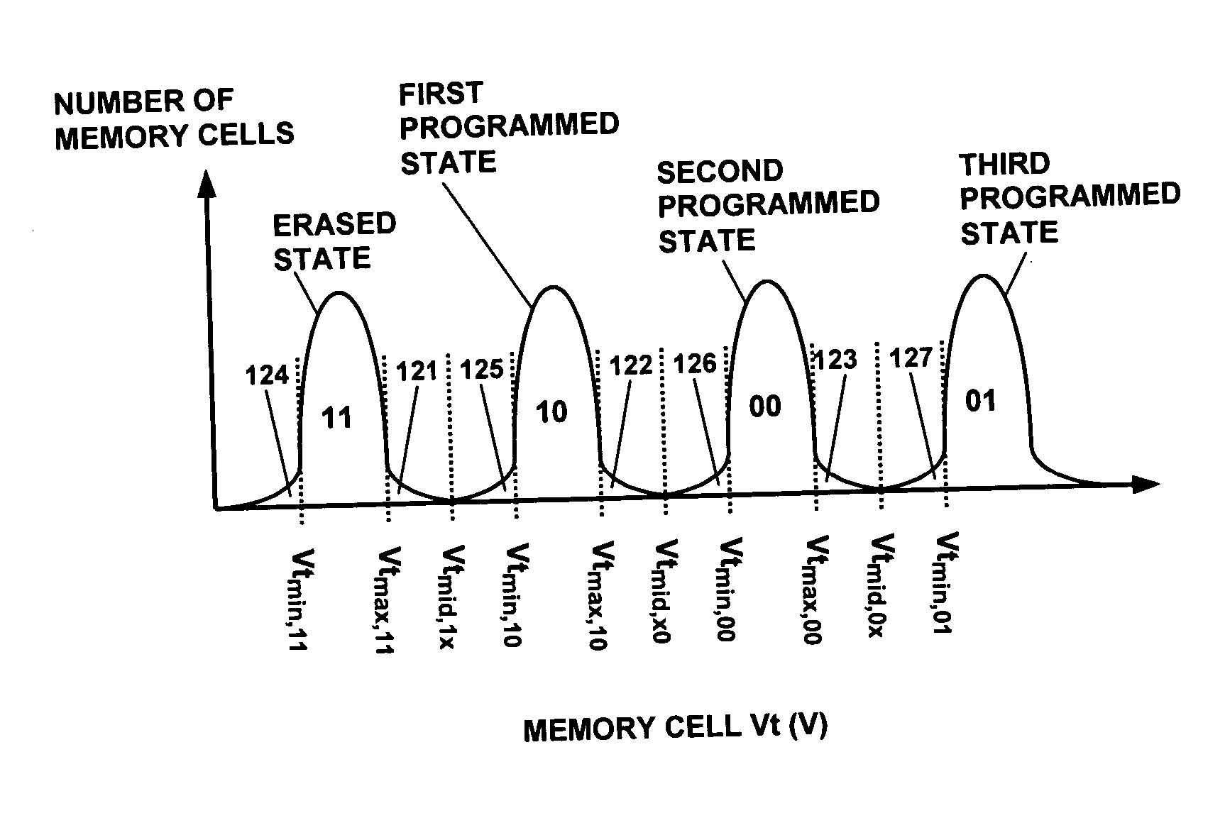
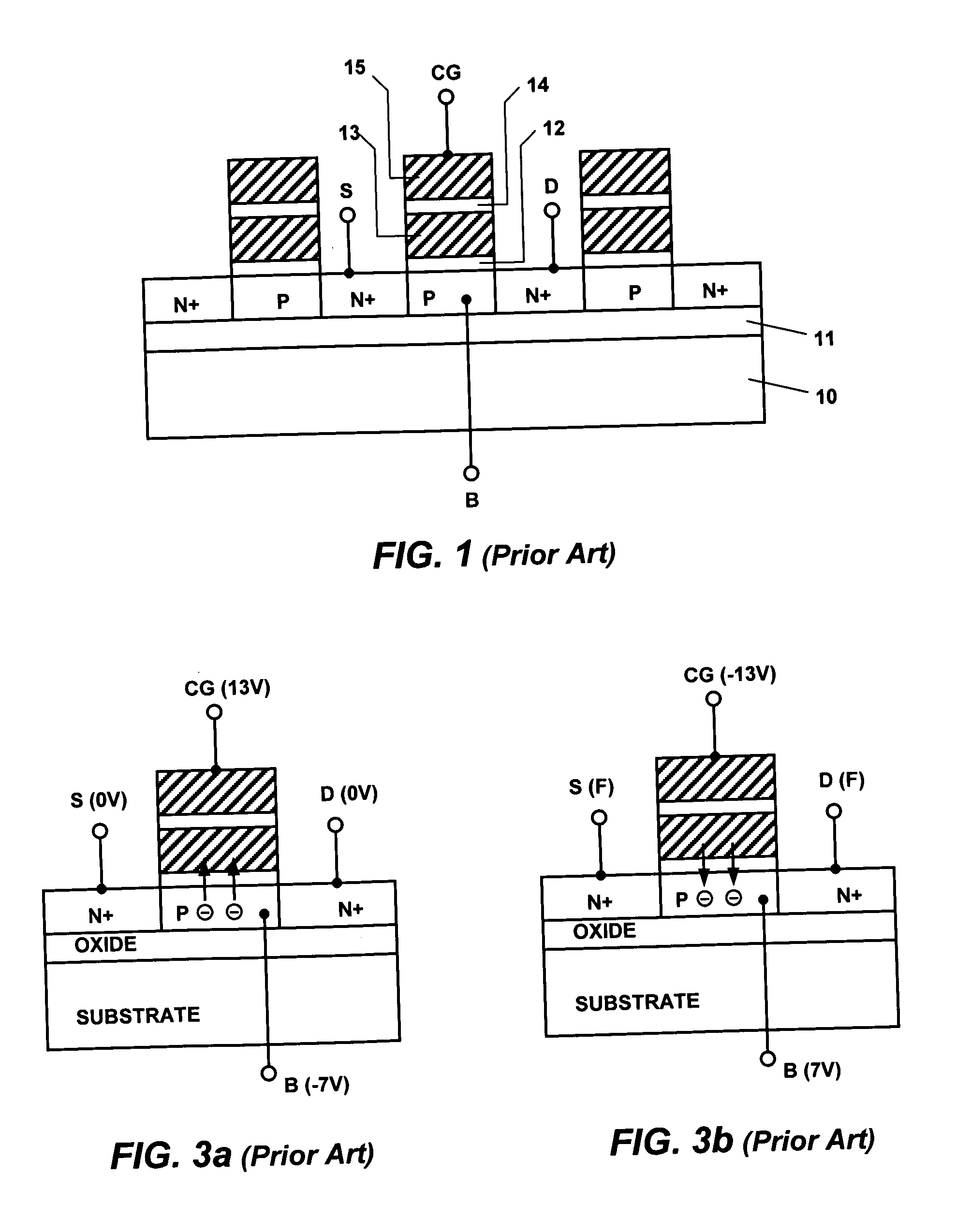
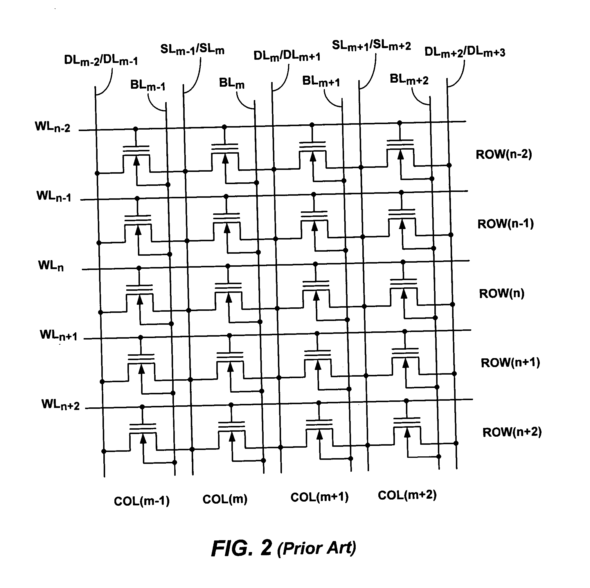
[0075] Reference will now be made in detail to the preferred embodiments of the invention, examples of which are illustrated in the accompanying drawings. While the invention will be described in conjunction with the preferred embodiments, it will be understood that they are not intended to limit the invention to these embodiments. On the contrary, the invention is intended to cover alternatives, modifications, and equivalents, which may be included within the spirit and scope of the invention as defined by the appended claims. Furthermore, in the following detailed description of the present invention, numerous specific details are set forth in order to provide a thorough understanding of the present invention. However, it will be obvious to one of ordinary skill in the art that the present invention may be practiced without these specific details. In other instances, well known methods, procedures, components, and circuits have not been described in detail as not to unnecessarily ...
PUM
 Abstract
Description
Claims
Application Information