Sensor and method for making same
- Summary
- Abstract
- Description
- Claims
- Application Information
AI Technical Summary
Problems solved by technology
Method used
Image
Examples
example
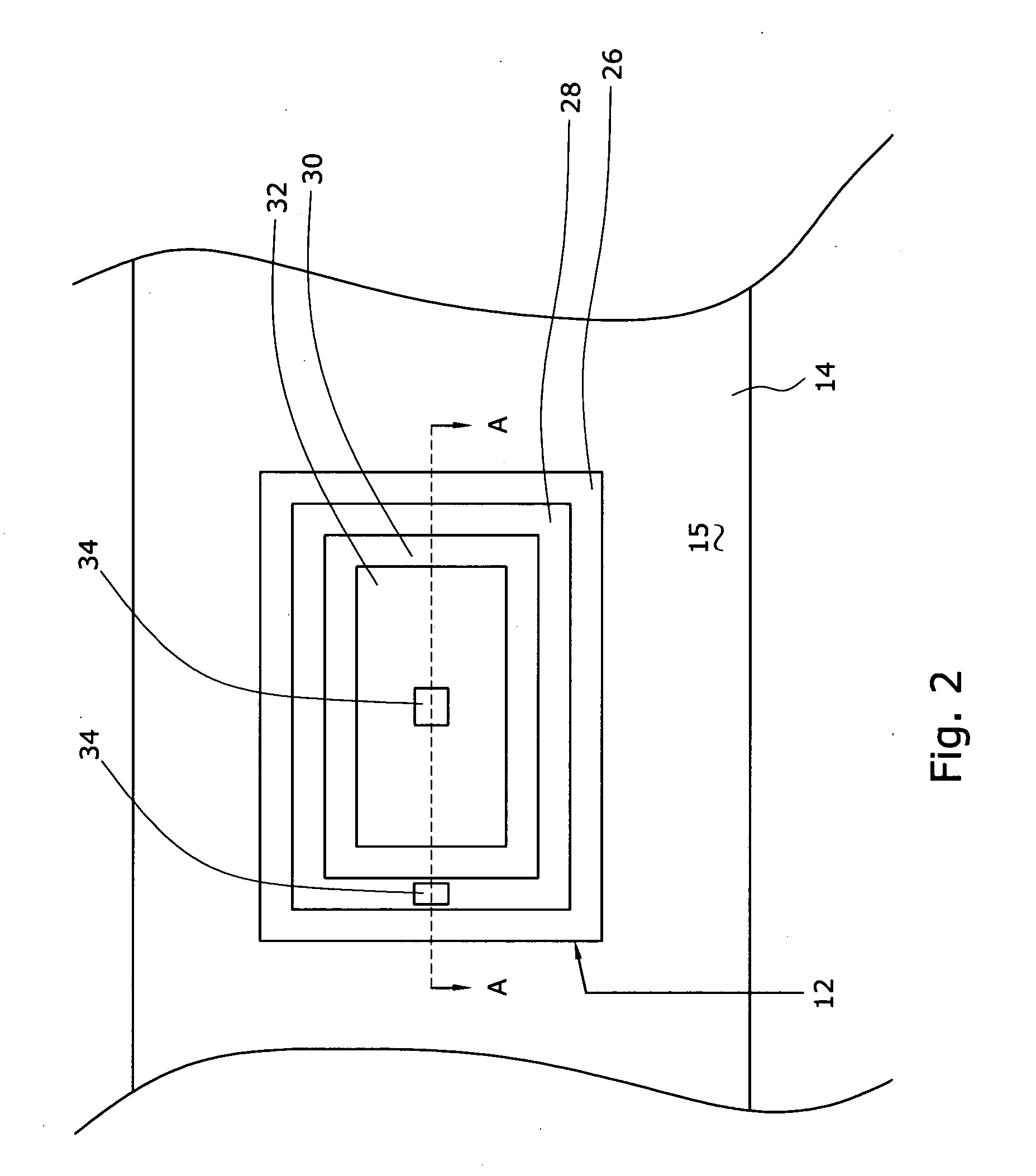
[0046] Following the preferred direct write and co-sintering procedure described above, several three-layer sandwich-printed and co-sintered thermistors were manufactured. The direct write deposition technology used was a robotic micropen system depositing onto an alumina substrate. All sensors were manufactured using platinum for the conductive layers (e.g., first and second conductive layers 28, 32 as described with respect to FIGS. 2, 3) and an yttrium chromite mixture as the thermistor layer (e.g., thermistor layer 30 as described with respect to FIGS. 2, 3). The layers were co-sintered in air for one (1) hour and then Ar for one (1) hour. A platinum ink was used to direct write the leads. The sensors were made in varying sizes. Table 1 lists the resistance of each of these thermistors at 25 degrees centigrade.
TABLE 1Inventive Thermistor Designation and Resistance at 25° C.DesignationResistance at 25° C. (kohms)IS#152IS#2145IS#319IS#4540
[0047] Each of these thermistors was cal...
PUM
 Abstract
Description
Claims
Application Information


