Method of controlling the film properties of a CVD-deposited silicon nitride film

a technology of silicon nitride and film properties, which is applied in the direction of coatings, chemical vapor deposition coatings, semiconductor devices, etc., can solve the problems of instability problems, inconvenient use of pecvd sinsub>x/sub>h dielectric films, and the a-si:h tfts with sinsub>x/sub>:h gate dielectric are said to have instability problems, etc., to achieve greater control

Inactive Publication Date: 2006-01-26
APPLIED MATERIALS INC
View PDF15 Cites 362 Cited by
  • Summary
  • Abstract
  • Description
  • Claims
  • Application Information

AI Technical Summary

Benefits of technology

[0023] We have discovered that adding H2 to a precursor gas composition including SiH4, NH3, and N2 is effective in improving the wet etch rate and wet etch rate uniformity of a-SiNx:H films across a substrate surface upon which said films have been PECVD deposited. As mentioned above, wet etch rate is an indi

Problems solved by technology

However, the a-Si:H TFTs with SiNx:H gate dielectric are said to have instability problems, such as the threshold voltage shift and the inverse subthreshold slope under a DC gate voltage bias.
Their instability problems are said to be caused by the high trap density in the SiNx: H film and the defects created at the a-Si:H/SiNx:H interface.
The authors claim that PECVD SiNx:H dielectric films are not useful as a gate insulator because they contain large amounts of bonded hydrogen (20%-40%) in the form of N—H and Si—H bonds.
As the size of flat panel displays increase, it becomes increasingly difficult to control the uniformity of the individual films produced across the increased surface area.
With respect to PECVD deposited silicon-nitride comprising films, which are used either as the gate dielectric layer or as the passivation dielectric layer, control of uniformi

Method used


Image

  • Method of controlling the film properties of a CVD-deposited silicon nitride film
  • Method of controlling the film properties of a CVD-deposited silicon nitride film
  • Method of controlling the film properties of a CVD-deposited silicon nitride film

Examples


example one

The Overall Process for Forming a TFT

[0054] To provide a general understanding of the relationship of the PECVD deposited a-SiNx:H gate dielectric film and the a-SiNx:H passivation dielectric film relative to the other components of the TFT, a brief description of the overall fabrication process of the TFT embodiment shown in FIG. 1 is presented below.

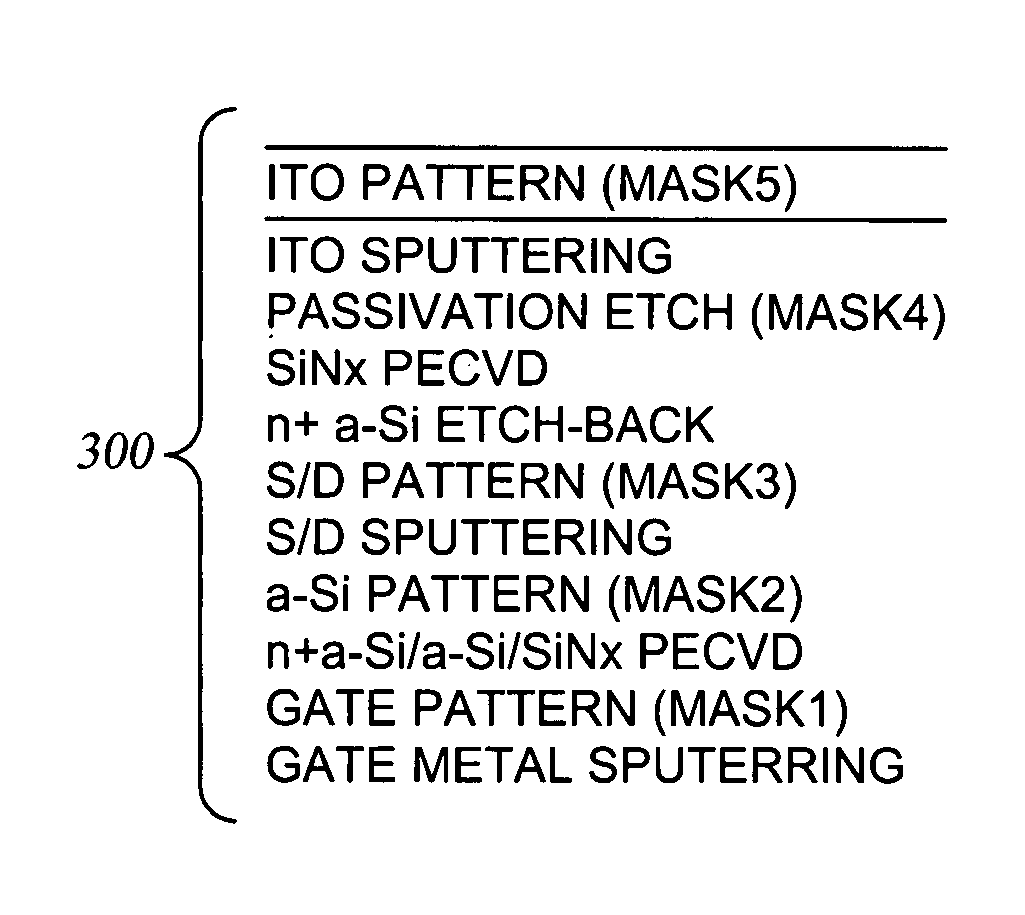
[0055]FIG. 3A show a series of process steps 300 which may be carried out to create the TFT device shown in FIGS. 3B and 3C. FIG. 3B provides a schematic side view of a substrate including a TFT structure. FIG. 3C provides a schematic top-view 336 of a substrate including several TFT structures.

[0056] In the first step, “Gate Metal Sputtering”, a conductive layer 302 is sputter deposited over a glass substrate 301 using techniques known in the art. In this particular instance, the substrate 301 is a glass substrate having a thickness of 0.7 mm. The conductive layer 302 is actually a bilayer, where the bottom portion of the layer is ...

example two

The Process for Depositing an a-SiNx:H Gate Dielectric Layer

[0067] We have previously described all of the performance requirements for the a-SiNx:H gate dielectric layer. We carried out extensive experimentation in an effort to produce a PECVD deposited a-SiNx:H gate dielectric layer which met the performance requirements, and which provided uniformity in terms of film thickness and film properties, including structural and chemical composition, when the gate dielectric layer is PECVD deposited over a large substrate surface area (larger than 1000 mm×1000 mm, for example).

[0068] The basic requirements for the a-SiNx:H film are that: the Si—H bonded content of the a-SiNx:H film is less than about 15 atomic %; the film stress ranges from 0 to about −1010 dynes / cm2; the refractive index (RI) of the film ranges from about 1.85 to about 1.95; and the wet etch rate in HF solution (Buffer Oxide Etchant 6:1) is less than 800 Å / min. In addition, the chemical composition of the film, in te...


PUM

PropertyMeasurementUnit
Temperatureaaaaaaaaaa

Abstract

We have discovered that adding H2 to a precursor gas composition including SiH4, NH3, and N2 is effective at improving the wet etch rate and the wet etch rate uniformity across the substrate surface of a-SiNx:H films which are deposited on a substrate by PECVD. Wet etch rate is an indication of film density. Typically, the lower the wet etch rate, the denser the film. The addition of H2 to the SiH4/NH3/N2 precursor gas composition did not significantly increase the variation in deposited film thickness across the surface of the substrate. The a-SiNx:H films described herein are particularly useful as TFT gate dielectrics in the production of flat panel displays. The uniformity of the film across the substrate enables the production of flat panel displays having surface areas of 25,000 cm2 and larger.

Description

BACKGROUND OF THE INVENTION [0001] 1. Field of the Invention [0002] The present invention pertains to a method of controlling the film properties of a silicon nitride film deposited by PECVD (plasma-enhanced chemical vapor deposition) over a substrate having a large surface area, and to the film deposited by the method. In particular, the uniformity of the density of the silicon nitride film across the substrate surface is improved by controlling the film-forming precursors. [0003] 2. Brief Description of the Background Art [0004] Current interest in thin film transistor (TFT) arrays is particularly high because these devices are used in liquid crystal active matrix displays of the kind often employed for computer and television flat panels. The liquid crystal active matrix displays may also contain light emitting diodes for back lighting. Further, organic light emitting diodes (OLEDs) have been used for active matrix displays, and these organic light emitting diodes require TFTs fo...

Claims


Application Information

Patent Timeline
IPC IPC(8): H01L21/469C23C16/00
CPCC23C16/345C23C16/5096H01L29/66765H01L29/4908H01L21/3185H01L21/02274H01L21/02208H01L21/0217
Inventor PARK, BEOM SOOCHOI, SOO YOUNGWON, TAE KYUNGWHITE, JOHN M.
Owner APPLIED MATERIALS INC
Why Eureka
Try Eureka