Substrate processing method
a processing method and substrate technology, applied in the direction of basic electric elements, electrical equipment, semiconductor devices, etc., can solve the problems of inability to predict the device lifetime with certainty, the increase of gate leakage current, and the inability to achieve reliability for the semiconductor devi
- Summary
- Abstract
- Description
- Claims
- Application Information
AI Technical Summary
Benefits of technology
Problems solved by technology
Method used
Image

Examples
first embodiment
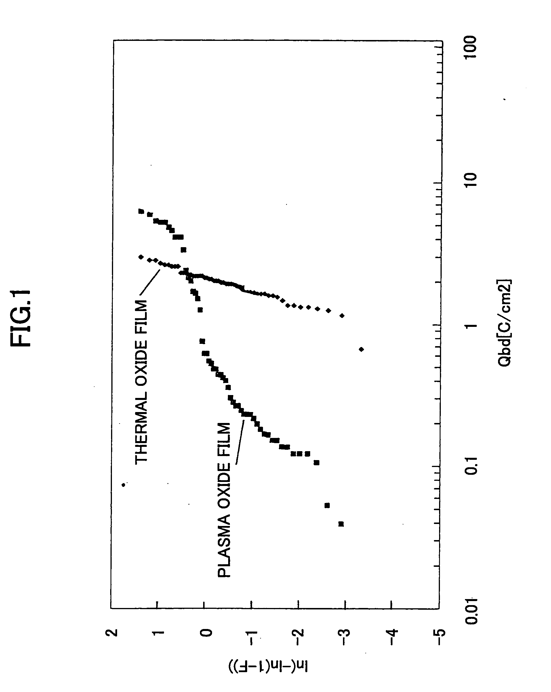
[0028] The inventor of the present invention has acquired the knowledge, in an experimental investigation on the formation process of oxide films, nitride films and oxynitride films on a silicon substrate by microwave plasma processing, suggesting that organic substance remaining on the silicon substrate surface exerts a significant effect on the reliability of insulation film formed on the substrate.
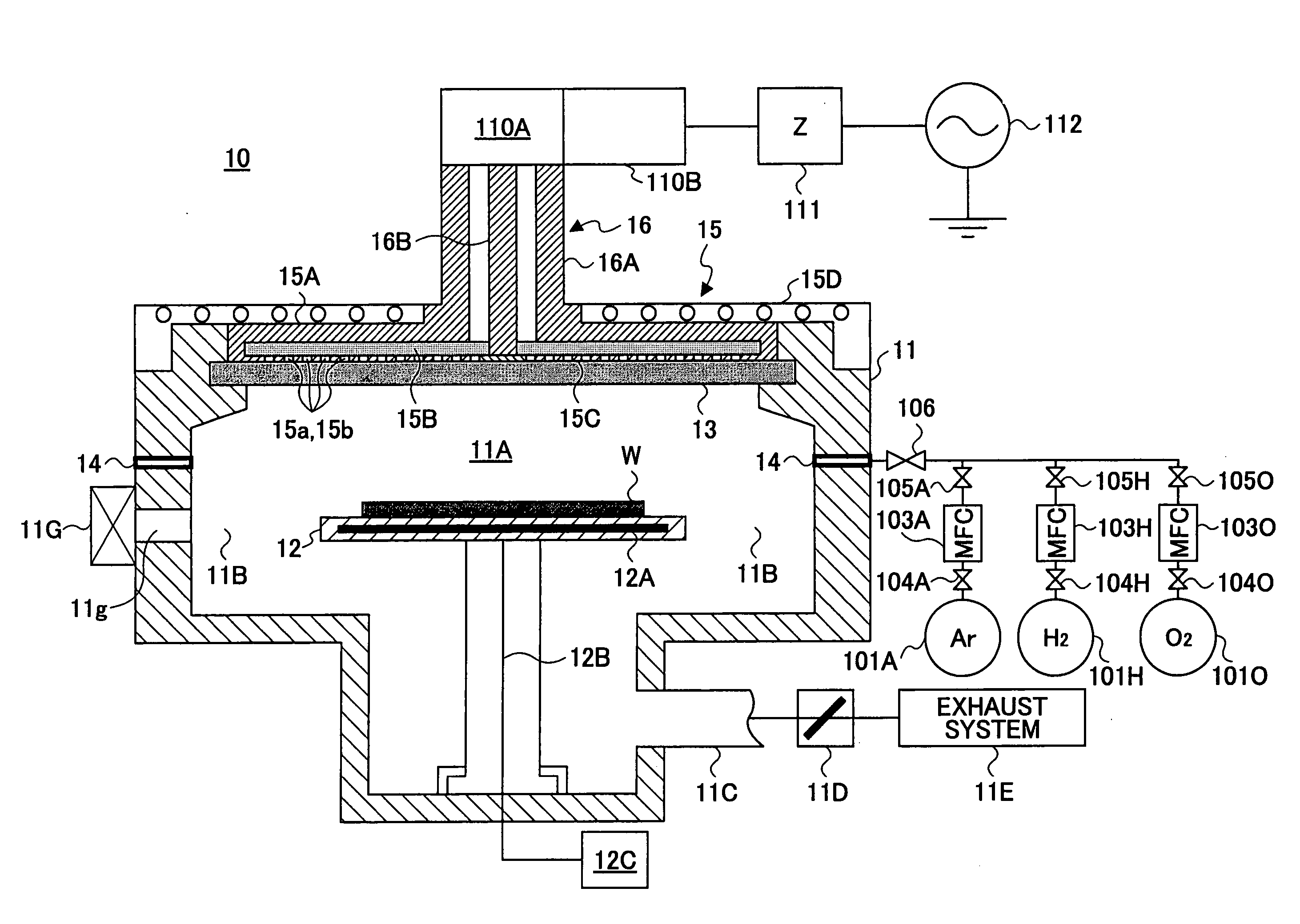
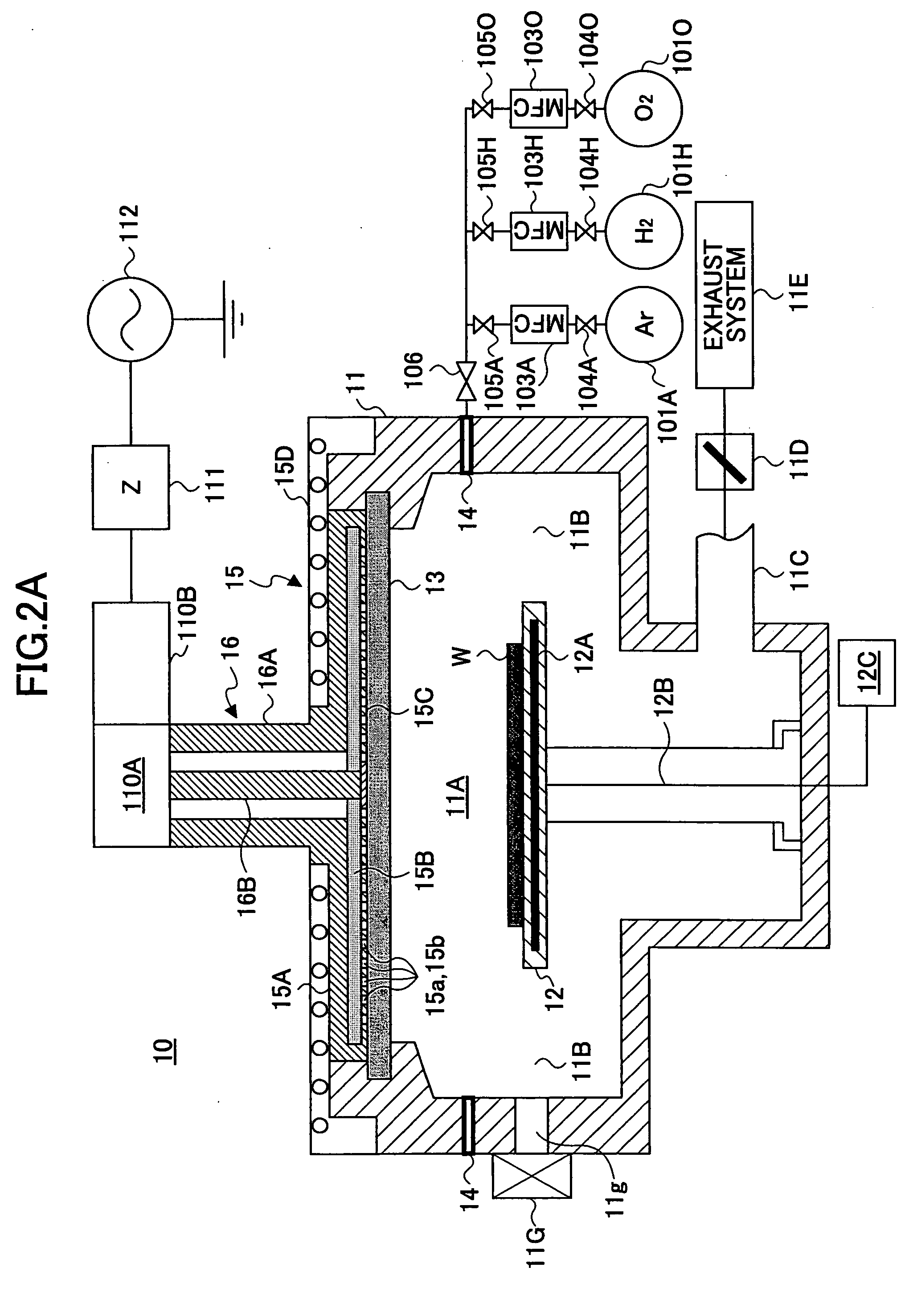
[0029]FIGS. 2A and 2B schematically show the construction a microwave plasma substrate processing apparatus 10 used by the inventor of the present invention.
[0030] Referring to FIG. 2A, the plasma substrate processing apparatus 10 includes a processing vessel 11 in which a processing space 11A is formed such that a stage 12 holding a substrate W to be processed thereon is formed in the processing space 11A, wherein the processing vessel 11 is evacuated by an evacuation system 11E at an evacuation port 11C via a space 11B surrounding the stage 12 and an adaptive pressure controller 11D...
second embodiment
[0060]FIGS. 6A and 6B show the substrate processing method according to a second embodiment of the present invention.
[0061] Referring to FIG. 6A, there is formed a silicon oxide film 22 on a silicon substrate 21 by the process of FIGS. 3A and 3B explained before or by other process, wherein the surface of the silicon oxide film 22 is processed by the mixture gas plasma of argon and hydrogen under the condition similar to the process of FIG. 3A, and the organic substance remaining on the surface of the silicon oxide film 22 is removed.
[0062] Next, in the step of FIG. 6B, there is caused a growth of the oxide film on the silicon oxide film 22 thus processed by applying the mixed gas plasma of argon and oxygen under the similar condition as FIG. 3B, and with this, there is formed an oxide film 25.
[0063] It should be noted that the oxide film 25 thus formed has excellent reliability and leakage current density similarly to the plasma oxide film that explained with the previous embodi...
third embodiment
[0066]FIGS. 7A shows the construction of an overall substrate processing system 100 that includes the substrate processing apparatus 10 of FIGS. 2A and 2B and used for the processing of the present invention of FIGS. 3A and 3B or FIGS. 6A and 6B, while FIG. 7B shows a computer used for controlling the substrate processing apparatus 10 of FIGS. 2A and 2B in the system of FIG. 8A.
[0067] Referring to FIG. 7A, the system 100 includes the Ar gas source 101A, the hydrogen gas source 101H and the oxygen gas source 1010, wherein the Ar gas source 101A supplies an Ar gas to the gas ring 14 of the substrate processing apparatus 10 via the mass flow controller 103A and via the valves 104A and 105A and further via the valve 106, while the hydrogen gas source 101H supplies a hydrogen gas to the gas ring 14 via the mass flow controller 103H and via the valves. 104H and 105H and further via the valve 106 coupled to the gas ring 14 commonly to the gas supply path of the Ar gas and the gas supply p...
PUM
| Property | Measurement | Unit |
|---|---|---|
| thickness | aaaaa | aaaaa |
| gate length | aaaaa | aaaaa |
| thickness | aaaaa | aaaaa |
Abstract
Description
Claims
Application Information
 - R&D
- Intellectual Property
- Life Sciences
- Materials
- Tech Scout
- Unparalleled Data Quality
- Higher Quality Content
- 60% Fewer Hallucinations
Browse by: Latest US Patents, China's latest patents, Technical Efficacy Thesaurus, Application Domain, Technology Topic, Popular Technical Reports.
© 2025 PatSnap. All rights reserved.Legal|Privacy policy|Modern Slavery Act Transparency Statement|Sitemap|About US| Contact US: help@patsnap.com