Selectively strained MOSFETs to improve drive current

a mosfet and drive current technology, applied in the direction of basic electric elements, electrical apparatus, semiconductor devices, etc., can solve the problems of limited success in strained sige implementation, and low cost of sige substrate implementation, so as to improve drive current and selectively introduce strain

Inactive Publication Date: 2006-02-02
TAIWAN SEMICON MFG CO LTD
View PDF4 Cites 54 Cited by
  • Summary
  • Abstract
  • Description
  • Claims
  • Application Information

AI Technical Summary

Benefits of technology

[0009] To achieve the foregoing and other objects, and in accordance with the purposes of the present invention, as embodied and broadly described herein, the present invention provides a MOSFET device pair with improved drive current and a method for producing the same to selectively introduce strain into a respective N-type and P-type MOSFET device channel region.
[0010] In a first embodiment, the method includes providing a first and second MOSFET device having a respective first polarity and second polarity opposite from the first polarity selected from the group consisting of P and N type on a semiconducting substrate; forming a first stressed nitride layer having a first stress type selected from the group consisting of compressive and tensile stress over the first and second MOSFET device active areas; removing the first stressed nitride layer overlying the second MOSFET device active area; forming a second stressed nitride layer having a second stress type opposite the first stress type over the first and second MOSFET device active areas; removing the second stressed nitride layer overlying the first MOSFET device active area; and, forming a dielectric insulating layer over the first and second MOSFET device active areas having a less compressive or tensile stress.

Problems solved by technology

However, several integration problems inherent in SiGe processing technology as well as the cost of SiGe substrates remain issues limiting the cost-effective implementation of strained SiGe approaches to gain the benefits of strain-induced band modification.
These approaches have met with limited success, however, since the formation of the stressed dielectric layer of a particular type of stress e.g., tensile or compressive, has a degrading electrical performance effect on a CMOS device with an opposite type of polarity e.g., N vs.
For example, as NMOS device performance is improved by forming tensile stressed dielectric layers, PMOS device performance is typically degraded.
Other shortcomings in prior art approaches are the adverse affect of the dielectric stressed layers on subsequent gap filling ability of a subsequently deposited dielectric layers as well as associated thermal processing temperatures which detrimentally affect previously formed materials such as stressed dielectric layers and metal silicides.
For example, typical processes of forming pre-metal dielectric (PMD) layers over stressed dielectric layers may lead to stress relaxation or thinning of stressed dielectric layers making device performance improvement, if any, unpredictable.
In addition, prior art processes in forming stressed dielectric layers have the limitation of requiring different processing tools for a given stress type, thereby increasing the cost of production and reducing throughput.
In addition, prior art approaches of forming stressed dielectric layers have been limited by the range of stress levels that may be formed, typically depending primarily on thickness to achieve a desired stress level.
When producing highly stressed dielectric layers, this approach has the offsetting effect of limiting a gap filling ability in a subsequent PMD layer deposition process thereby leading to the formation of voids, compromising device yield and reliability.

Method used


Image

  • Selectively strained MOSFETs to improve drive current
  • Selectively strained MOSFETs to improve drive current
  • Selectively strained MOSFETs to improve drive current

Examples


Embodiment Construction

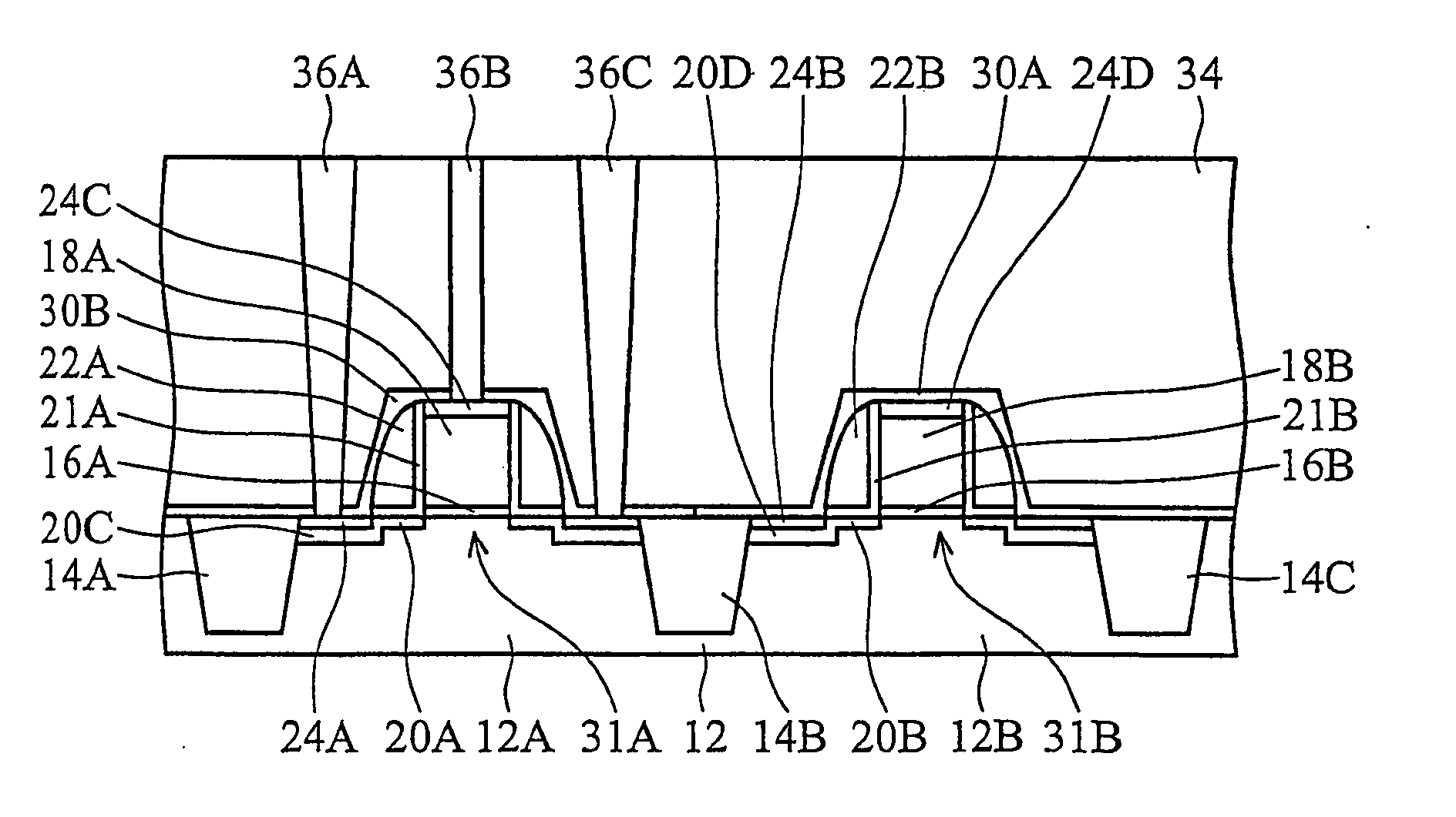
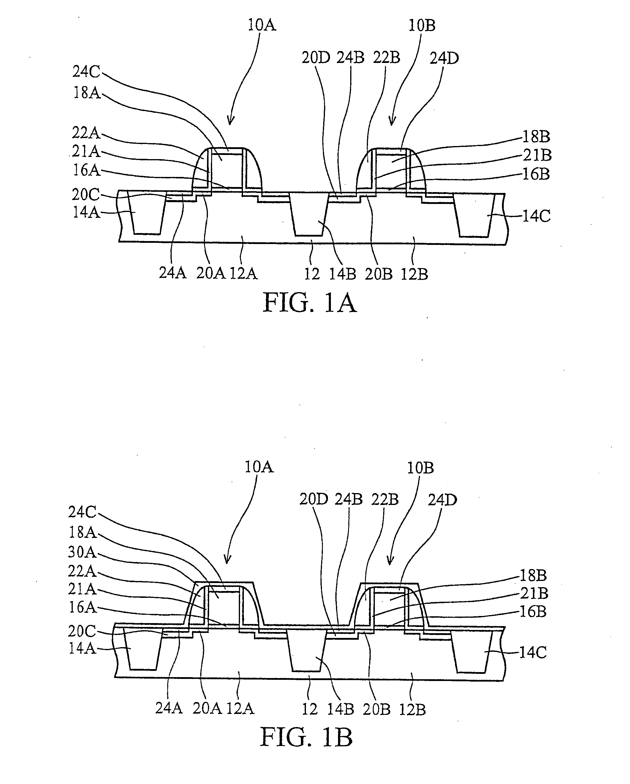
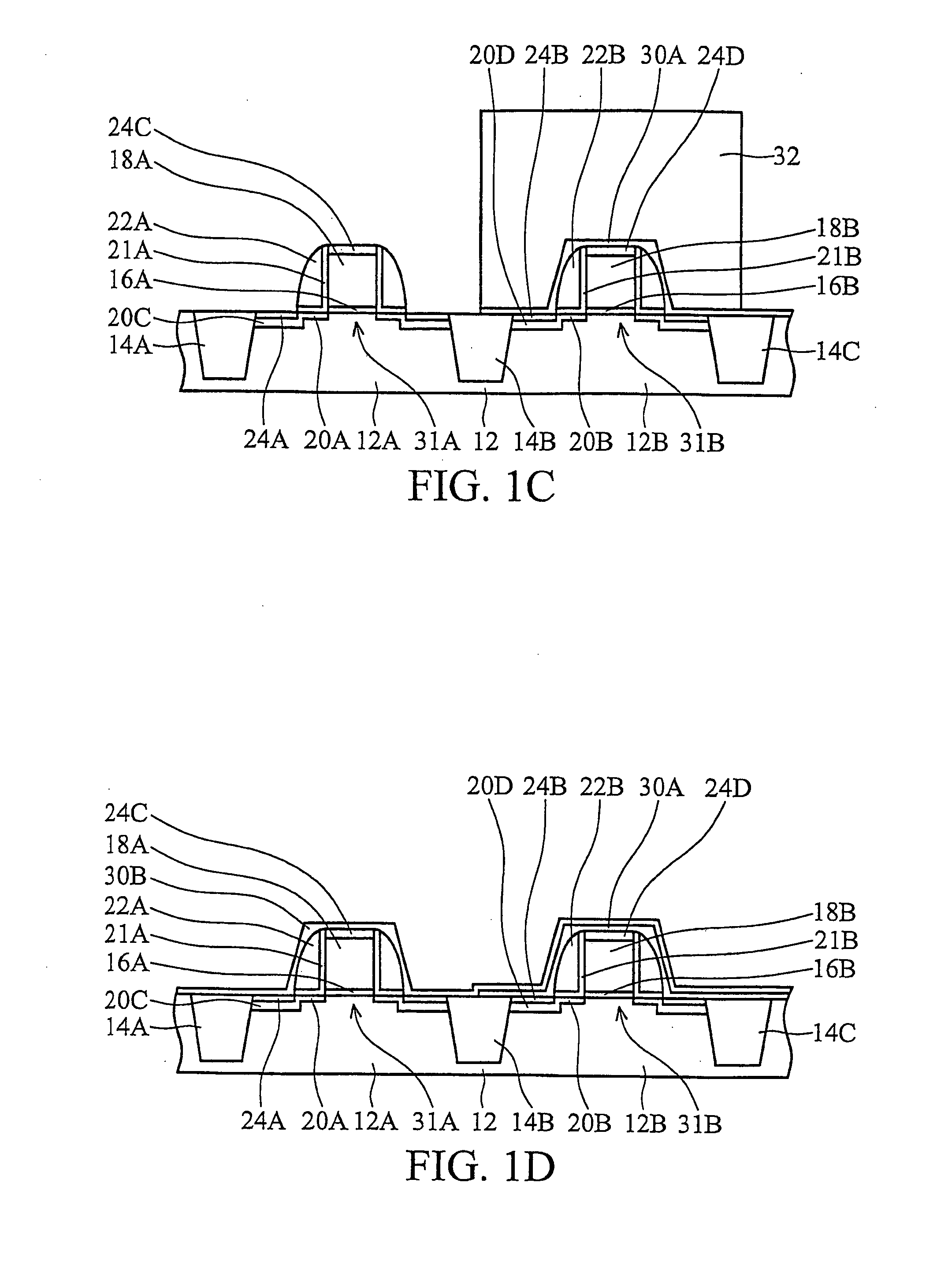
[0015] Although the method of the present invention is explained with reference to exemplary NMOS and PMOS MOSFET devices, it will be appreciated that the method of the present invention may be applied to the formation of any MOSFET device where a strain is controllably introduced into a charge carrier channel region by selective formation of stressed dielectric layers overlying the respective NMOS and / or PMOS device regions with subsequent preferred PMD layer formation.

[0016] Referring to FIGS. 1A-1F in an exemplary embodiment of the method of the present invention, are shown cross-sectional schematic views of a portion of a semiconductor wafer during stages in production of MOSFET structures including NMOS and PMOS devices 10A and 10B. For example, referring to FIG. 1A, is shown a semiconductor substrate 12, which may include silicon, strained semiconductor, compound semiconductor, multi-layered semiconductors, silicon on strained semiconductor, silicon on insulator, and combinat...


PUM

PropertyMeasurementUnit
frequencyaaaaaaaaaa
temperatureaaaaaaaaaa
thicknessaaaaaaaaaa

Abstract

A MOSFET device pair with improved drive current and a method for producing the same to selectively introduce strain into a respective N-type and P-type MOSFET device channel region, the method including forming a compressive stressed nitride layer on over the P-type MOSFET device and a tensile stressed nitride layer on the N-type MOSFET device followed by forming a PMD layer having a less compressive or tensile stress.

Description

FIELD OF THE INVENTION [0001] This invention generally relates to formation of MOSFET devices in integrated circuit manufacturing processes and more particularly to MOSFET devices and methods of forming the same to selectively provide strain-induced charge carrier band modification for enhanced charge carrier mobility and improved MOSFET device drive current. BACKGROUND OF THE INVENTION [0002] Mechanical stresses are known to play a role in charge carrier mobility which affects drive current and Voltage threshold shifts. The effect of mechanical stresses is to induce a strain on a MOSFET channel region and thereby improve a MOSFET device drive current which is proportional to charge carrier mobility. [0003] Generally, various manufacturing processes are known to introduce strain into the MOSFET device channel region. For example, strain may be introduced into the channel region by the use of selectively strained SiGe substrates. However, several integration problems inherent in SiGe...

Claims


Application Information

Patent Timeline
Patent Type & Authority Applications(United States)
IPC IPC(8): H01L21/8238H01L21/31
CPCH01L21/3185H01L29/7843H01L29/7842H01L21/823807H01L21/02274H01L21/0214H01L21/0217
Inventor FU, CHU-YUNCHANG, CHENG-HUNG
Owner TAIWAN SEMICON MFG CO LTD
Why Eureka
Try Eureka