Enhanced passgate structures for reducing leakage current

a passgate structure and leakage current technology, applied in the field of integrated circuit devices, can solve the problems of reducing leakage current, high leakage current, and difficult design hurdles to overcome, and achieve the effects of reducing leakage current, high speed operation, and increasing the vt of the passgate structur

Inactive Publication Date: 2006-02-09
ALTERA CORP
View PDF33 Cites 6 Cited by
  • Summary
  • Abstract
  • Description
  • Claims
  • Application Information

AI Technical Summary

Benefits of technology

[0009] In one arrangement, leakage current is reduced and high speed operation is maintained by raising the VT of the passgate structure above that of the VT of other structures (e.g., logic transistors) and by applying a passgate activation voltage that is higher than a nominal voltage (e.g., “low” system voltage) to the gate of the passgate structure. An advantage realized by increasing the VT of the pass-gate structures is that it reduces the leakage current when the passgate structures are turned OFF. The pass-gate activation voltage is sufficient to enable the pass-gate structure to operate at a desired speed even though the VT has been increased relative to the VT of other structures other than the passgate structures.
[0010] Because the passgate activation voltage is higher than the nominal voltage, the power source providing the activation voltage may be used to power configurable memory cells such as SRAM. Powering the configurable memory cells with a voltage higher than the nominal voltage reduces the soft-error-rate because the higher voltage increases the critical charge needed to flip the cell.

Problems solved by technology

With the current trend in scaling down device geometries (e.g., 0.18 μm process down to 0.13 μm, 90 nm, and lower) and the consequent use of ever-lower operating voltages (e.g., supply voltages, bias voltages, etc.), which are nearing levels comparable to VT, the ability of transistor passgate structures to function at relatively high speeds while at the same time minimizing leakage current is a difficult design hurdle to overcome.
Moreover, this trend of smaller device geometries and consequent use of lower operating voltages is creating a design tradeoff between speed (e.g., response time for the passgate transistor to turn ON) and leakage current (e.g., the current that passes through the passgate transistor when turned OFF) that was not previously experienced with larger device geometries and the consequent use of higher operating voltages.
That is, if conventional design techniques are applied to smaller device geometries, high speed passgate operation is accompanied with high leakage current, whereas low leakage current is accompanied with low speed passgate operation.
High leakage current is undesirable because it results in excess heat, power loss, and poorer performance.
Another problem associated with shrinking geometries is the consequent use of lower operating voltages.
This lower operating voltage is typically a nominal voltage supplied to the integrated circuitry, and may be insufficient for certain circuitry, such as configurable memory cells (e.g., SRAM) within the integrated circuitry, to operate properly.

Method used


Image

  • Enhanced passgate structures for reducing leakage current
  • Enhanced passgate structures for reducing leakage current
  • Enhanced passgate structures for reducing leakage current

Examples


Embodiment Construction

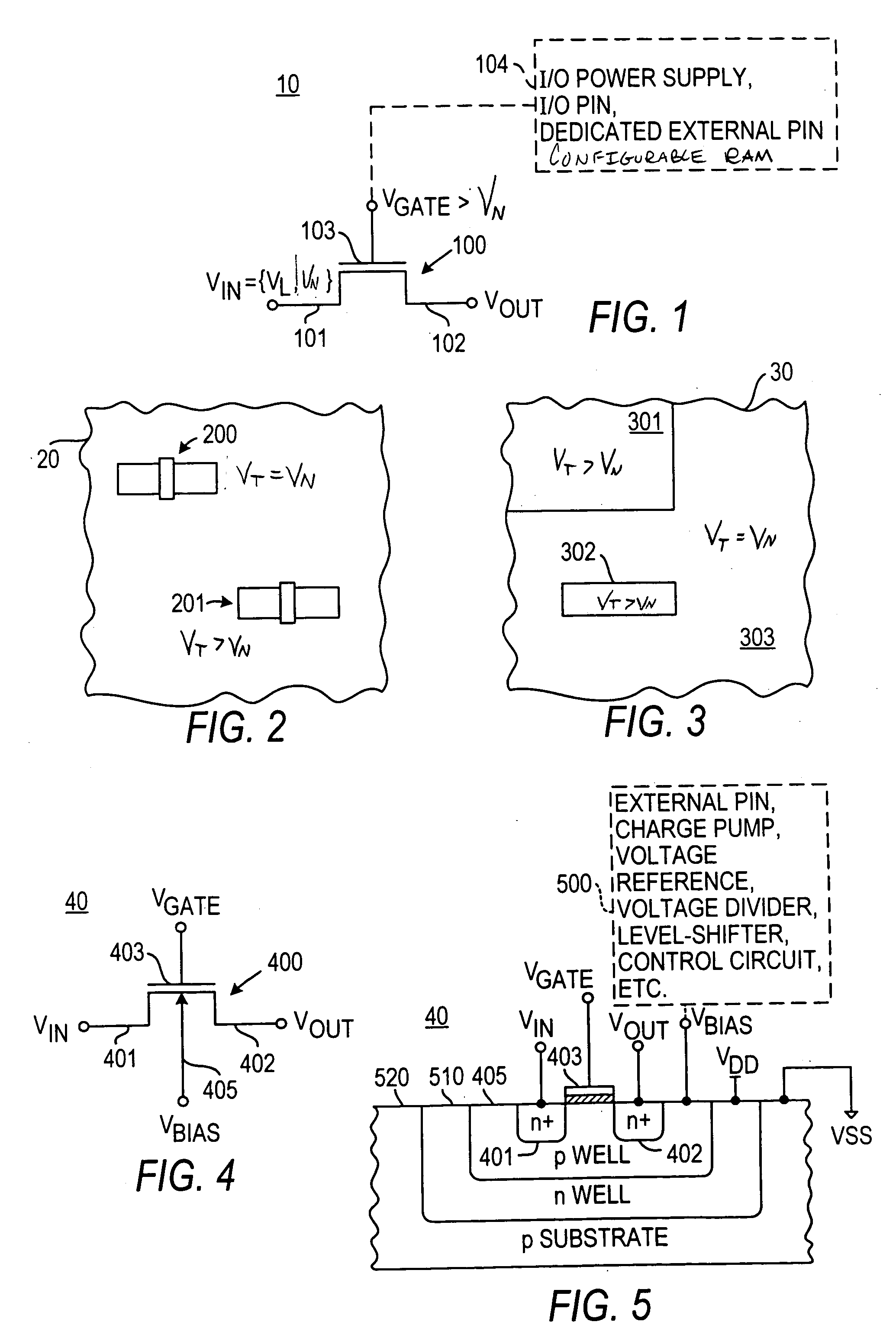
[0023] For the purpose of simplifying the discussion of the principles of the present invention, the techniques and embodiments described herein will focus on NMOS passgates. However, the principles illustrated herein are applicable to similar arrangements involving PMOS pass-gates.

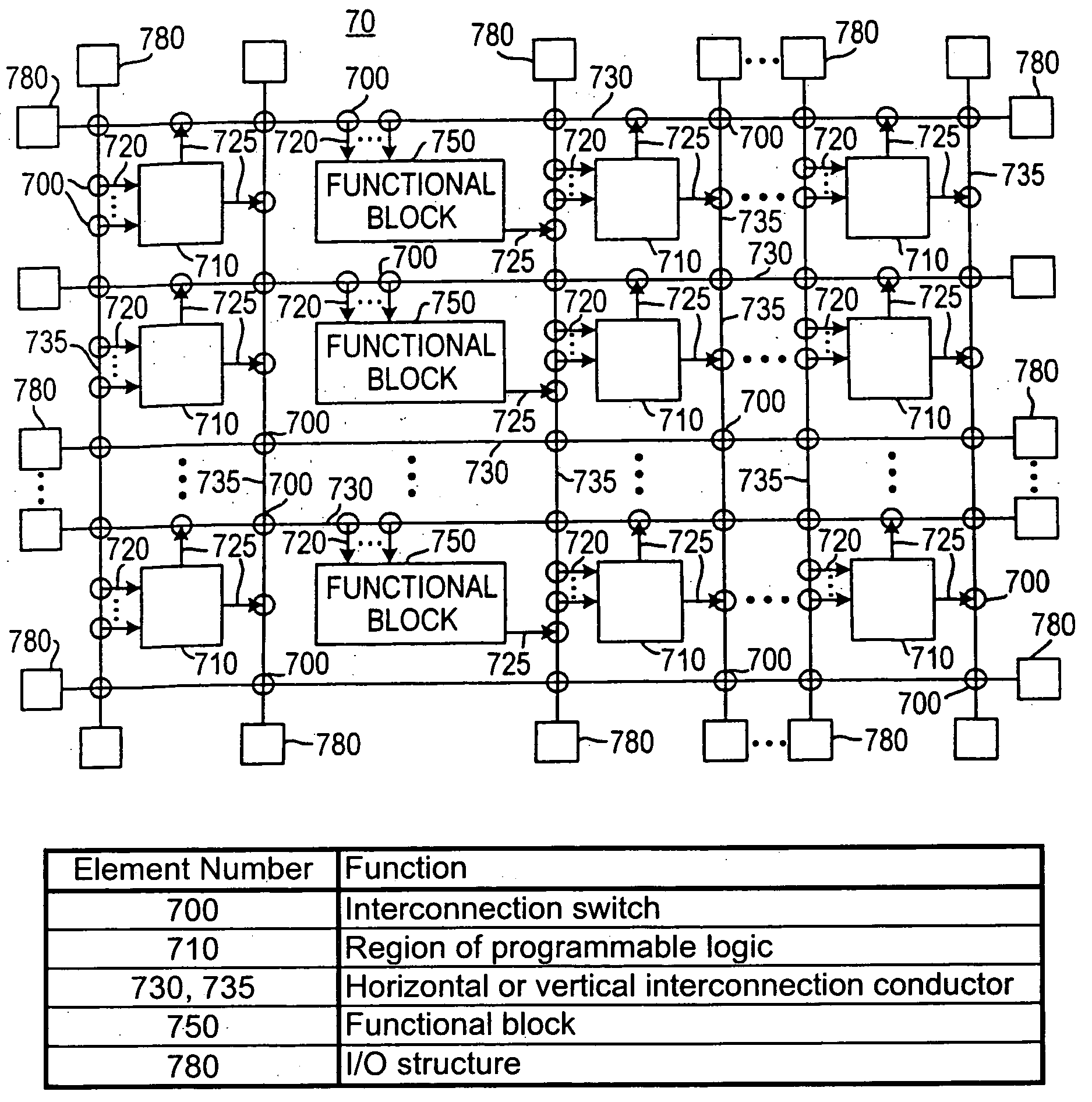
[0024] As defined herein, a nominal voltage is the voltage that is used predominately throughout an integrated circuit, such as a programmable logic device, and is typically associated with “low” voltages. The nominal voltage is sometimes referred to as a system voltage or a core circuitry voltage.

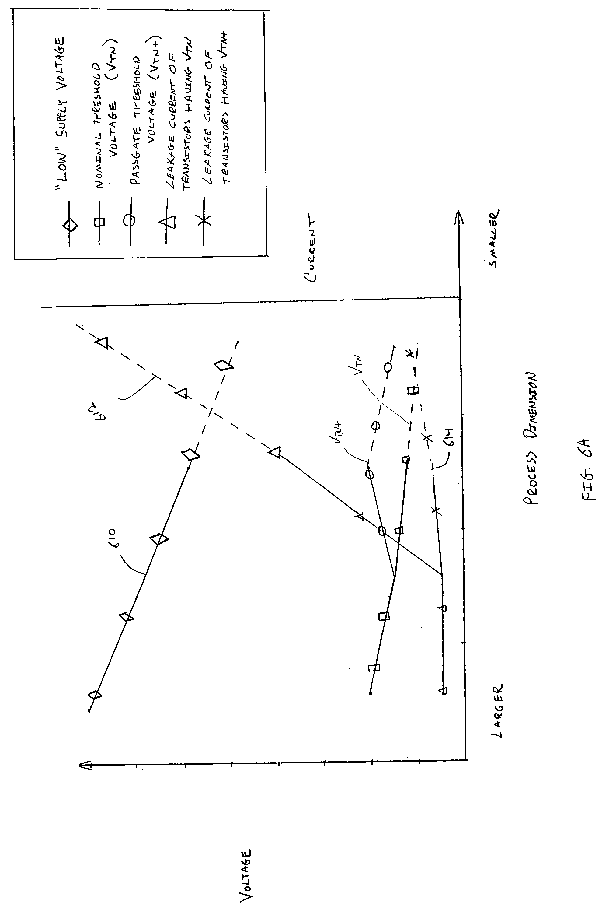
[0025] As defined herein, a nominal threshold voltage is the threshold voltage of transistors other than the passgate transistors according to the invention that are included in the integrated circuitry (e.g., programmable logic device). A nominal VT may be the VT of a transistor (e.g., a logic transistor) fabricated using a particular process (e.g., a 90 nm process) without attempting to produce a VT that wou...


PUM


Abstract

Enhanced passgate structures for use in low-voltage systems are presented in which the operational speed of the passgate structures is maximized, while minimizing leakage current when the structure is turned “OFF.” In one arrangement, the VT of the pass-gate structures is increased relative to the VT of other transistors fabricated according to a particular process dimension. In addition, a passgate activation voltage is applied to the passgate structures such that the passgate activation voltage is higher in voltage than a nominal voltage being supplied to circuitry other than the passgate structures.

Description

BACKGROUND OF THE INVENTION [0001] This invention relates to integrated circuit devices, and more particularly to the pass-gate structures that may be used in such devices. [0002] One of the most ubiquitous structures within an integrated circuit device is the single-transistor passgate, which is commonly used to implement (either singly or in combination with other circuits) switches, multiplexers, logic functions (e.g., pass transistor logic), and gating mechanisms for tristatable circuits (e.g., buffers and drivers). In some integrated circuit devices, single-transistor passgate structures may account for a significant portion of the circuitry; for example, in the case of programmable logic devices, single-transistor passgates are used extensively throughout the device as part of the programmable interconnection circuitry. [0003] The operation of a typical single-transistor passgate may be succinctly illustrated by a description of an NMOS passgate (analogous principles of operat...

Claims


Application Information

Patent Timeline
Patent Type & Authority Applications(United States)
IPC IPC(8): H03K19/173
CPCH03K19/1778H03K19/17792H03K19/17784
Inventor LUI, HENRY Y.KABANI, MALIKPATEL, RAKESHHOANG, TIM TRI
Owner ALTERA CORP
Why Eureka
Try Eureka