Semiconductor integrated circuit having built-in PLL circuit

a technology of integrated circuits and semiconductors, applied in the field of phase locked loops, can solve the problems of difficult integration of the capacitive element cb>1/b> itself on the chip, and achieve the effects of preventing an increased phase error of the pll loop, less temperature dependence, and increasing side-band spuriousness

Inactive Publication Date: 2006-02-09
RENESAS ELECTRONICS CORP
View PDF9 Cites 9 Cited by
  • Summary
  • Abstract
  • Description
  • Claims
  • Application Information

AI Technical Summary

Benefits of technology

[0014] It is an object of the present invention to provide a loop filter which comprises a second- or higher order filter including capacitive elements, the capacitance ratio of which can be reduced, allowing the integration of the loop filter on a chip.
[0025] Also, the voltage regulator, which does not include a reference voltage generator circuit, will not adversely affect the charge pump or transmission VCO. Even if the voltage generated by the voltage regulator has temperature dependency, the switching element is controlled by the output signal from the temperature detector circuit to switch the generated voltage in accordance with the detected temperature, making it possible to supply the charge pumps and transmission VCO with a voltage with less temperature dependency.

Problems solved by technology

Such a second-order filter employs two capacitive elements, wherein a loop filter for a transmission PLL handles relatively high frequencies, causing the larger capacitive element C1 to have a high capacitive value on the order of nF (nanofarad), which makes it difficult to integrate the capacitive element C1 itself on a chip.

Method used


Image

  • Semiconductor integrated circuit having built-in PLL circuit
  • Semiconductor integrated circuit having built-in PLL circuit
  • Semiconductor integrated circuit having built-in PLL circuit

Examples


first embodiment

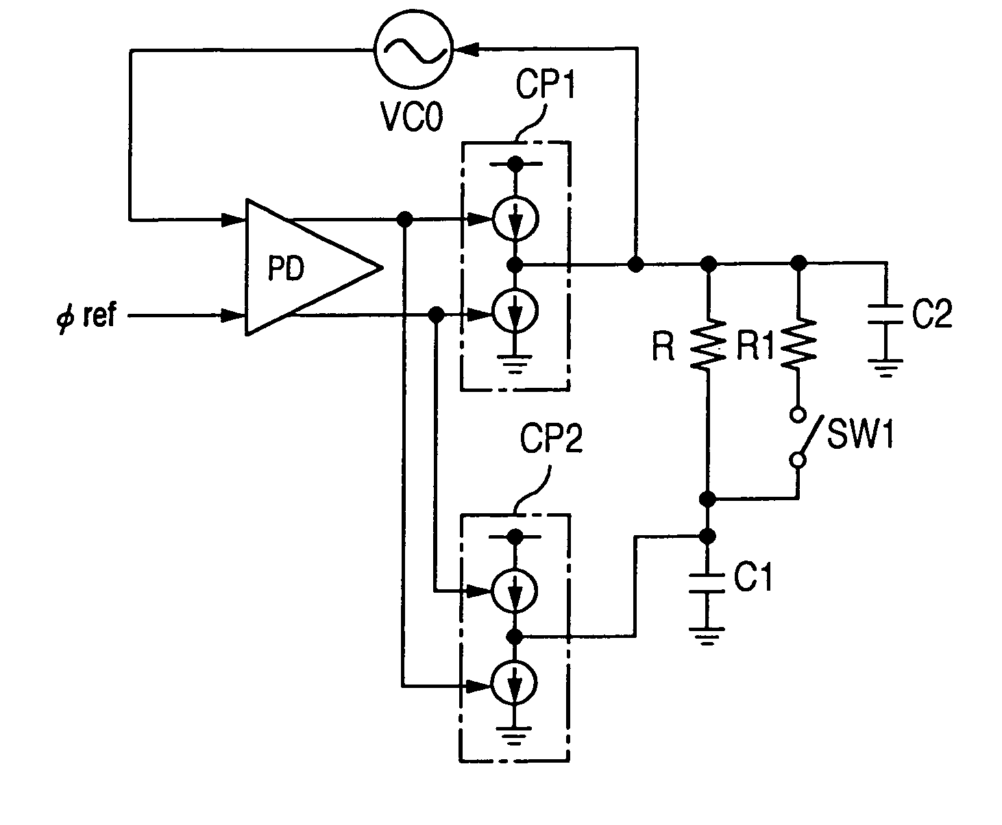
[0044]FIG. 6 illustrates one embodiment of a loop filter which can be provided on a PLL loop. The loop filter in this embodiment comprises a first charge pump CP1 which is made up of regulated current sources I11, I12, and switches SW11, SW12 connected in series with the regulated current sources I11, I12, respectively; a capacitor C2 connected between an output node N1 of the charge pump CP1 and a ground point; a resistor R and a capacitor C1 connected between the output node N1 and ground point in parallel with the capacitor C2; and a second charge pump CP2 which is made up of regulated current sources I21, I22, and switches SW21, SW22 connected in series with the regulated current sources I21, I22, respectively, and has an output node N2 connected to a connection node N3 at which the resistor R is connected to the capacitor C1.

[0045] In the loop filter (FIG. 6) of this embodiment, the switch SW21 for charging the second charge pump CP2 is controlled on / off by a down signal DOWN ...

second embodiment

[0058] Generally, the voltage controlled oscillator (VCO) suffers from a varying oscillation frequency as the supply voltage fluctuates. To prevent the varying oscillation frequency, the present invention supplies a transmission oscillator circuit (TXVCO) with a supply voltage from a voltage regulator. FIG. 10 illustrates one embodiment of a voltage regulator for supplying a transmission oscillator circuit (TXVCO) with a supply voltage.

[0059] The voltage regulator illustrated in FIG. 10 comprises a regulator unit 110 for generating a desired supply voltage using a base-emitter voltage Vbe of a bipolar transistor; and a temperature detector unit 120 for generating a control signal to the regulator unit 110. Conventional voltage regulators typically have a band gap reference circuit. The use of the band gap reference circuit permits the voltage regulator to generate a stable supply voltage without source voltage dependency regardless of changes in temperature. However, in a particula...

third embodiment

[0082]FIG. 14 illustrates one embodiment of a phase comparator circuit which is applied with the voltage from the voltage regulator in the foregoing embodiment for operations. The phase comparator circuit 236 in this embodiment comprises a signal comparator unit (left-hand side circuit) 361 and an output unit (right-hand side circuit) 362. As illustrated in FIG. 14, the signal comparator unit 361 comprises a cascaded configuration of differential circuits, wherein a current regulating transistor Q30 is connected to emitters of a lower differential transistor pair Q31, Q32, and differential transistor pairs Q33, Q34 and Q35, Q36 are connected to collectors of the lower differential transistor pair Q31, Q32. The transistors Q33, Q35 have their collectors coupled to each other, which are then connected to a common load transistor Q37. Likewise, the transistors Q34, Q36 also have their collectors coupled to each other, which are connected to a common load transistor Q38.

[0083] In this ...


PUM


Abstract

A semiconductor integrated circuit having a built-in PLL circuit which has two charge pump circuits for charging and discharging capacitive elements of a loop filter in response to signals generated by a phase comparator circuit. One of the two charge pump circuits has current sources which generate current values smaller than those generated by current sources of the other charge pump circuit. The loop filter has a first capacitive element connected to a charge / discharge node, and a second capacitive element connected to the charge / discharge node through a resistive element. The first capacitive element is charged and discharged by the one charge pump circuit, while the second capacitive element is charged and discharged by the other charge pump circuit. A charging current source of the one charge pump circuit operates simultaneously with a discharging current source of the other charge pump circuit, i.e., the charge pump circuits operate in opposite phase.

Description

CROSS-REFERENCE TO RELATED APPLICATION [0001] The present application relates to subject matters described in a co-pending application serial No. 10 / 253,922 filed on Sep. 25, 2002 assigned to the assignee of the present application. The disclosures of the co-pending application are incorporated herein by reference.BACKGROUND OF THE INVENTION [0002] The present invention relates to a phase locked loop (PLL) including a voltage controlled oscillator (VCO) circuit, and more particularly to techniques which are effectively applied to incorporation of a loop filter on a PLL into a semiconductor chip. More specifically, the present invention relates to techniques which are effectively utilized for a transmission PLL loop in a high frequency semiconductor circuit, for example, used in radio communication devices such as a portable telephone for modulating and upconverting a transmission signal. [0003] A radio communication device (mobile communication device) represented by a portable tele...

Claims


Application Information

Patent Timeline
Patent Type & Authority Applications(United States)
IPC IPC(8): H03L7/06H03L7/093H03L7/00H03L7/087H03L7/089H03L7/107
CPCH03L7/087H03L7/0893H03L7/1075H03L7/107H03L7/1072H03L7/0898
Inventor KIMURA, YASUYUKISHIMIZU, SATOSHIYOKOTA, MASAKATSUSUYAMA, KENDEC, ALEKSANDER
Owner RENESAS ELECTRONICS CORP
Why Eureka
Try Eureka