Information storage device, information storage method, and information storage program

a technology of information storage which is applied in the field of information storage device, information storage method, and information storage program, can solve the problems of low processing speed, low processing speed, and limited time for operation assurance of common sdram, and achieve the effect of high processing speed

Inactive Publication Date: 2006-02-09
SONY CORP
View PDF4 Cites 21 Cited by
  • Summary
  • Abstract
  • Description
  • Claims
  • Application Information

AI Technical Summary

Benefits of technology

[0016] The information storage method according to the present invention makes an address comparison. Therefore, it is possible to select the operations that can be simultaneously processed within the same clock. The optimum operations are selected in accordance with the address comparison result. The selected operations can be simultaneously processed within the same clock so that a high processing speed is attained.

Problems solved by technology

A common SDRAM is limited in terms of time for operation assurance.
Further, latency and real-time limitations are imposed on command issuance.
If a command is issued without such a wait, the operation is not guaranteed.
Therefore, even if a command can be issued on each clock, most of the clock period is vacant and unnecessary for operations.
As a result, the performance of the SDRAM deteriorates.

Method used


Image

  • Information storage device, information storage method, and information storage program
  • Information storage device, information storage method, and information storage program
  • Information storage device, information storage method, and information storage program

Examples


Embodiment Construction

[0025] An SDRAM (Synchronous Dynamic Random Access Memory or Synchronous DRAM) will now be described with reference to the accompanying drawings as one embodiment of an information storage device according to the present invention.

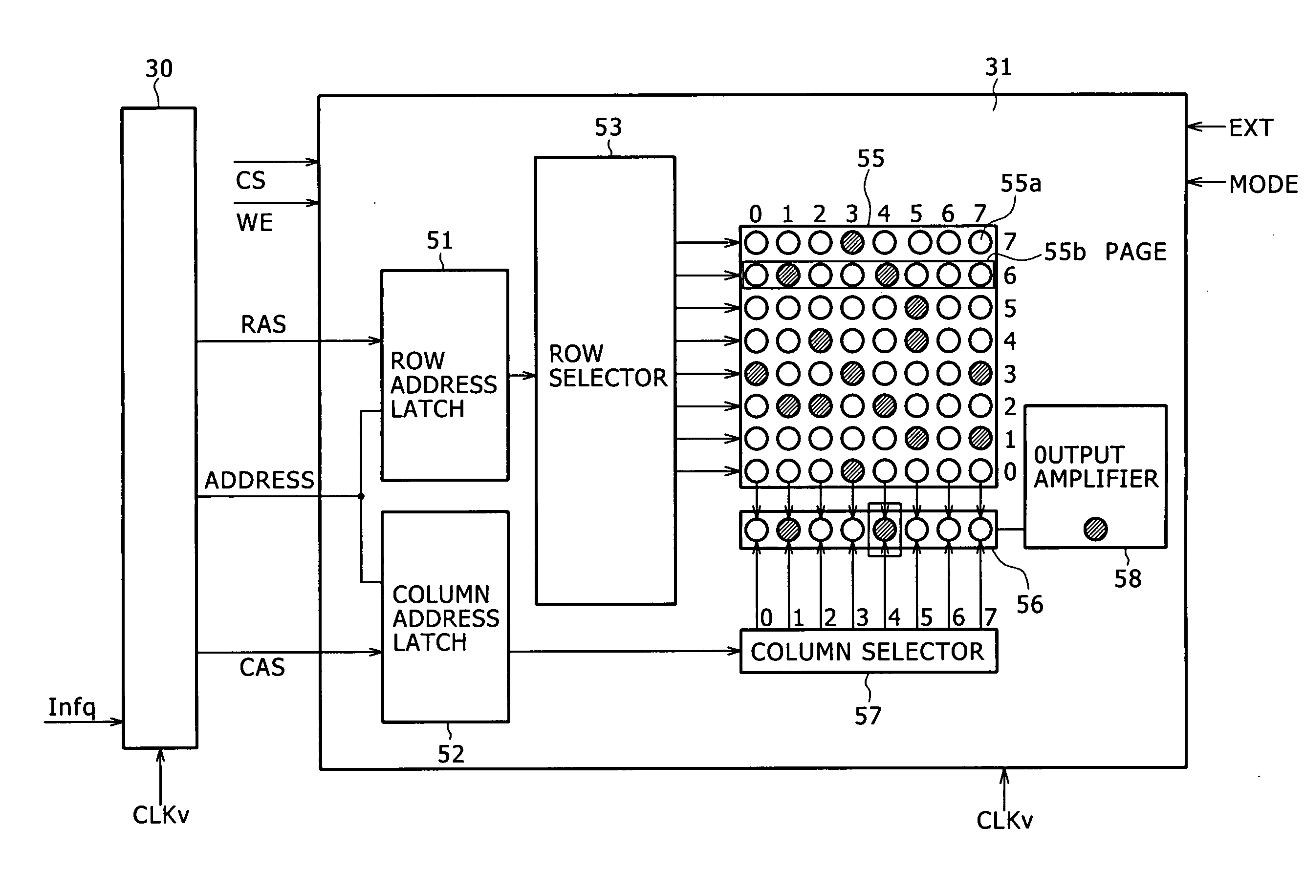
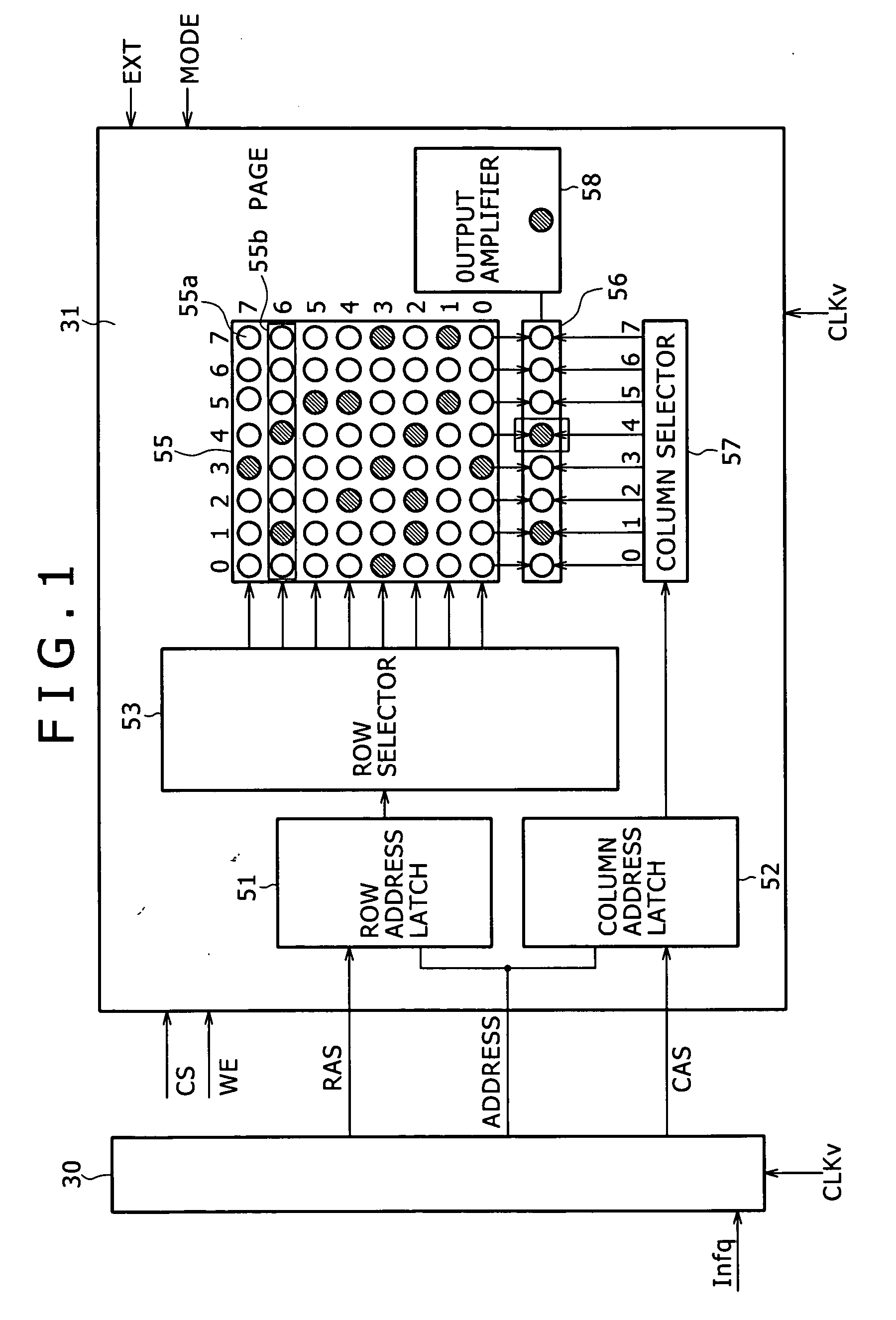
[0026]FIG. 1 is a block diagram illustrating a memory unit 31 according to the present embodiment and a memory controller 30, which is provided to transmit a control signal to the memory unit 31. The memory unit 31 is constructed as an SDRAM so that a variable clock signal CLKv is supplied from a required frequency control section.

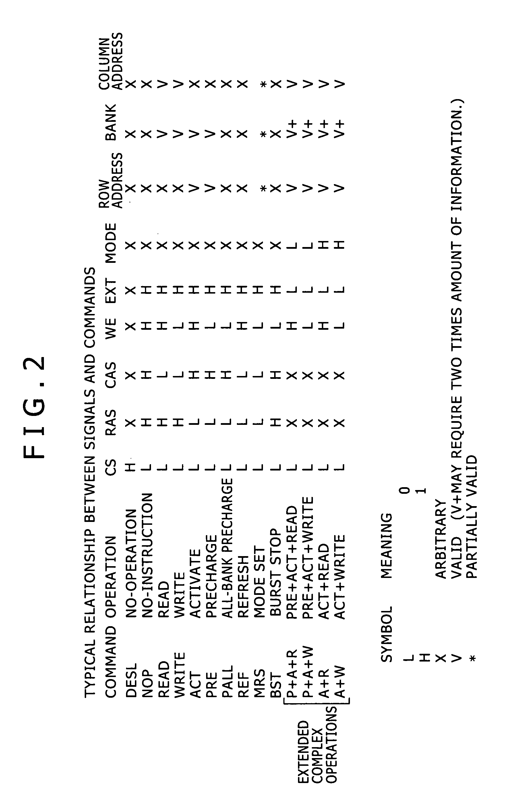
[0027] The memory controller 30 is a device that outputs control signals to control the operation of the memory unit 31, which is a DRAM. The present embodiment outputs not only an address signal and various control signals such as CS (chip select), RAS (row address strobe), CAS (column address strobe), WE (write enable), CKE (clock enable), BA (bank), column address, and row address, but also an EXT (extension) signal and MODE...


PUM


Abstract

Disclosed is a synchronous information storage device that uses a synchronizing clock signal to exercise operation timing control and processes operations with high efficiency to improve performance and provide low power consumption, which is characteristic of DRAMs. The information storage device includes a plurality of memory cells for storing data by accumulating an electrical charge and an amplifier for amplifying the electrical charge of the memory cells, and uses a synchronizing clock signal for input/output timing of the data. An electrical charge removal operation for moving an electrical charge from the memory cells to the amplifier or an electrical charge accumulation operation for acquiring an electrical charge from the amplifier and accumulating the electrical charge in the memory cells and an input/output operation for the amplifier in relation to the outside of the information storage device are processed while using a single clock of the synchronizing clock signal for synchronization timing.

Description

TECHNICAL FIELD [0001] The present invention relates to an information storage device that stores data by accumulating an electrical charge, and more particularly to a synchronous information storage device that achieves synchronization with a clock signal. BACKGROUND ART [0002] A DRAM (Dynamic Random Access Memory) is widely used as an information storage device that serves as a main memory for a personal computer or like system. Among others, an SDRAM (Synchronous Dynamic Random Access Memory or Synchronous DRAM), which is faster than a previously used, asynchronous DRAM, has been increasingly used. The SDRAM is a memory device that synchronizes its operation with a base clock frequency. Timing recognition is properly accomplished because it is in synchronism with a clock signal. Due to such timing recognition, the SDRAM operates rapidly. The SDRAM can transmit data with high efficiency particularly in a situation where data is continuously output in synchronism with a system cloc...

Claims


Application Information

Patent Timeline
Patent Type & Authority Applications(United States)
IPC IPC(8): G11C29/00G11C11/401G11C7/06G11C7/10G11C11/403G11C11/407G11C11/4091
CPCG06F2212/3042G11C7/065G11C2207/2245G11C11/40607G11C11/4091G11C7/1072G11C7/22G11C11/4076
Inventor SHIMOYAMA, TAKESHI
Owner SONY CORP
Why Eureka
Try Eureka