Eureka AIR delivers breakthrough ideas for toughest innovation challenges, trusted by R&D personnel around the world.

Method of fabricating a gate oxide layer

Inactive Publication Date: 2006-02-09
POWERCHIP SEMICON CORP
View PDF3 Cites 7 Cited by
  • Summary
  • Abstract
  • Description
  • Claims
  • Application Information

AI Technical Summary

Benefits of technology

[0011] The present invention provides a method for fabricating a gate oxide layer, wherein dopants are implanted into the substrate to lower the oxidation rate of the gate oxide layer that is being formed on the substrate. A thinning of the gate oxide layer is thereby prevented to increase the reliability of the device.
[0012] The present invention further provides a fabrication method for a gate oxide layer, wherein the thickness of the gate oxide layer remains uniform at the border between the substrate and the shallow trench isolation structure to prevent a generation of leakage current in the device.
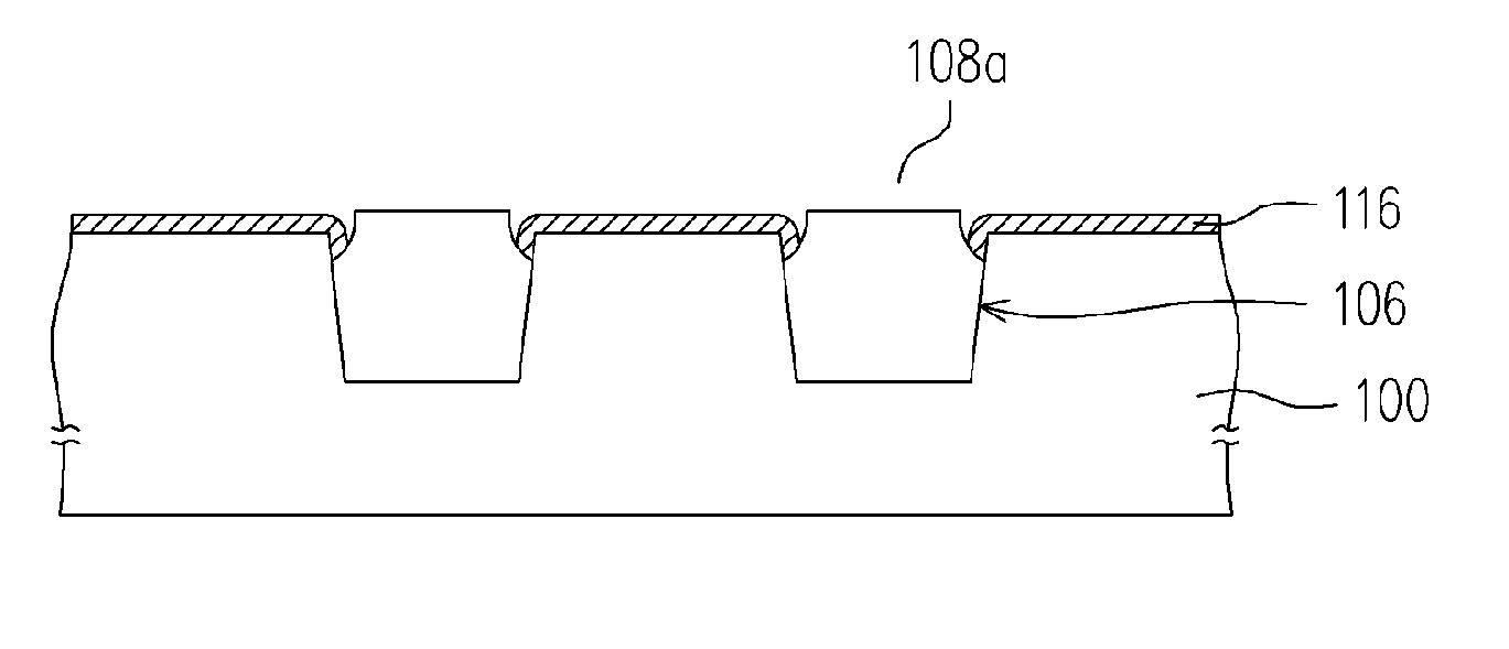
[0014] In accordance to an embodiment of the invention, the present invention provides an isolation structure with a spacer as a mask for the implantation of the nitrogen ions into the substrate in order to lower the growth grate of silicon oxide. As a result, the oxidation rate at the top edge corner of the trench and the oxidation rate at the central region of the substrate are substantially the same. A gate oxide layer with a uniform thickness is thus formed on the substrate to prevent the generation of leakage current in a device and to improve the reliability of the device.
[0016] In accordance to another embodiment of the invention, during the process in removing a portion of the mask layer, spacer is directly formed on the sidewall of the insulation layer to simplify the fabrication process and to reduce the production cost.
[0017] Further, the insulation layer (isolation structure) with the spacer on the sidewall can serve as a mask for the implantation of the nitrogen ions in order to lower the growth rate of silicon oxide. The oxidation rate at the top edge corner of the trench is thus substantially the same as the oxidation rate at the central part of the active region. A gate oxide layer with a uniform thickness is thus formed to prevent a thinning of the gate oxide layer and to improve the reliability of the device.

Problems solved by technology

As the integration of devices continues to increase, the isolation between devices becomes an important issue.
The LOCOS technique, however, encompasses many drawbacks, which include the generation of stress and the formation of bird's beak near the peripheral of the isolation structure.
As a result, a LOCOS isolation structure can not be used for an effective isolation of miniature devices.
However, during the fabrication process of the shallow trench isolation structure, removing the pad oxide layer and the mask layer with isotropic etching will lead to the formation of dents at the top edge corner of the shallow trench isolation structure.
The abnormal kink effect lowers the quality of devices and yields of the process.
Further, in the subsequent formation of the gate oxide layer, the oxidation rate is greatly affected by the dents at the top edge corner of the shallow trench isolation structure.
Consequently, the gate oxide layer formed at the top edge corner of the shallow trench isolation structure is thinner than the gate oxide layer formed at the active region, and a gate oxide layer with a non-uniformed thickness is resulted.
A thinning of a gate oxide layer will lower the reliability of the memory device.

Method used


Image

  • Method of fabricating a gate oxide layer
  • Method of fabricating a gate oxide layer
  • Method of fabricating a gate oxide layer

Examples


Embodiment Construction

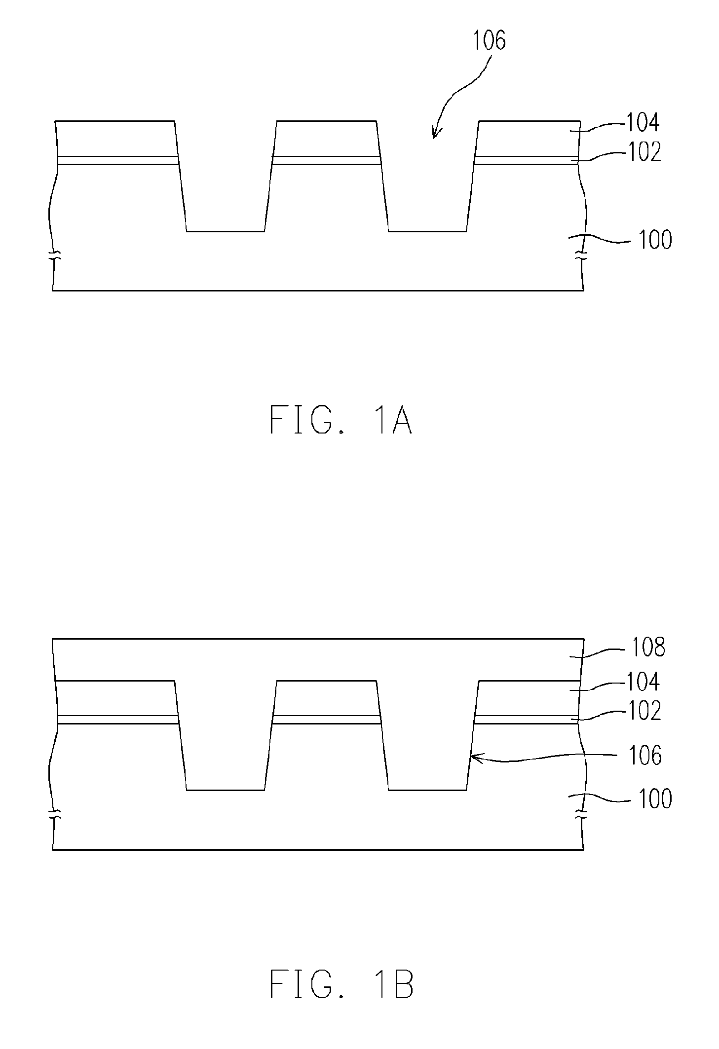
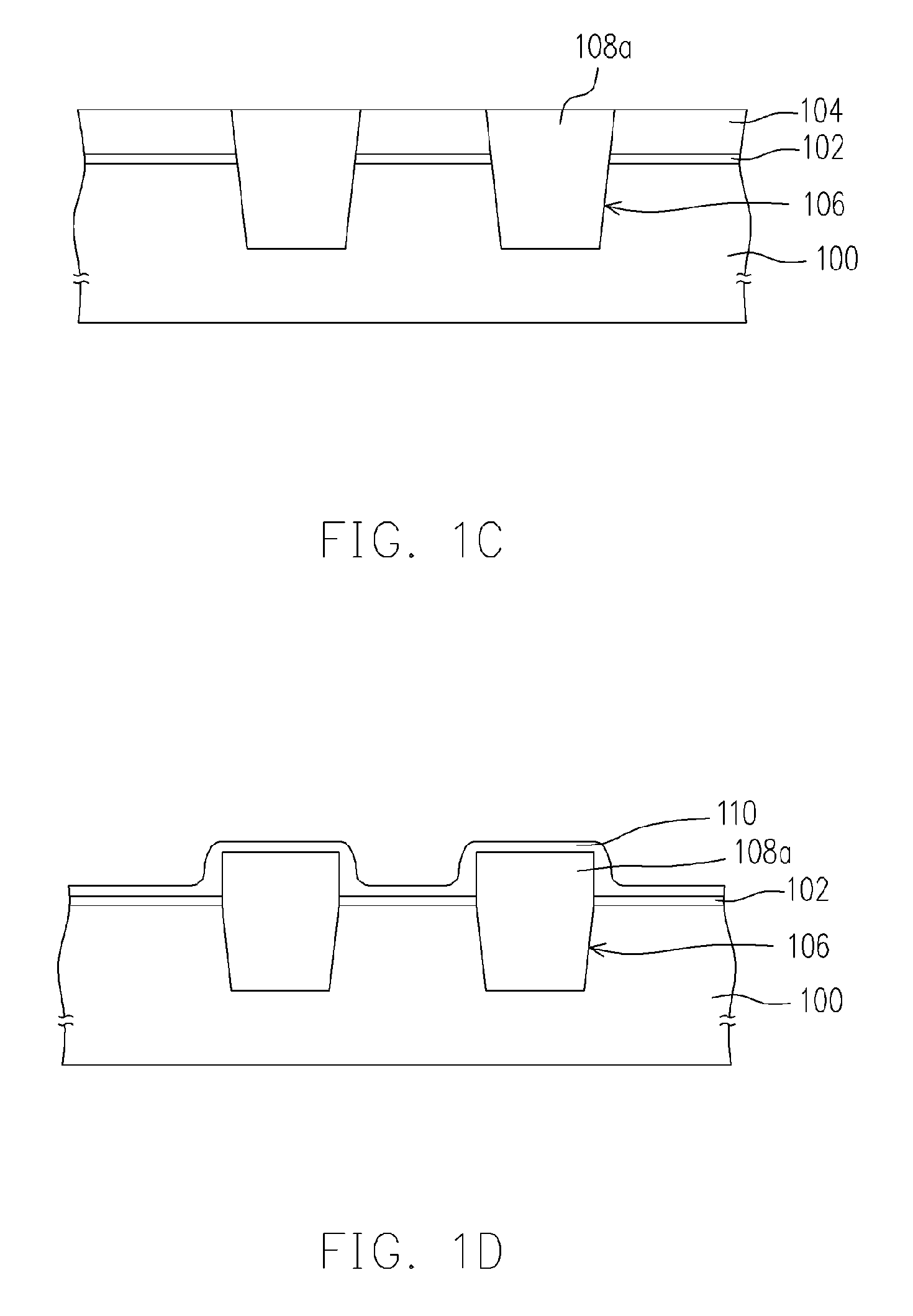
[0022]FIGS. 1A to 1G are schematic, cross-sectional view diagrams of a part of a semiconductor device for illustrating the fabrication process for a gate oxide layer according to one embodiment of the present invention.

[0023] Referring to FIG. 1A, a substrate 100, for example, a silicon substrate, is provided. A pad oxide layer 102 is formed on the substrate 100. A material used in forming the pad oxide layer 102 is, but not limited to, silicon oxide. The pad oxide layer 102 is formed by thermal oxidation, for example. The pad oxide layer 102 serves to protect the substrate 100 underneath from being damaged due to stress generated from the subsequently formed mask layer (silicon nitride layer).

[0024] A mask layer 104 is then formed on the pad oxide layer 102. The mask layer 104 is formed with, but not limit to, a silicon nitride material. The mask layer 104 is formed by chemical vapor deposition (CVD), for example. A photoresist layer (not shown) is further formed to cover the sub...


PUM


Abstract

A method of fabrication a gate oxide layer includes providing a substrate and an isolation structure on the substrate so as to isolate an active region. A spacer is formed on the sidewalls of the isolation structure. Using the isolation structure having the spacer as a mask, a dopant is implanted into the substrate for reducing the oxidation rate of the substrate. Thereafter, the spacer and a portion of the isolation structure are removed and an oxidation process is performed to form a gate oxide layer with a uniform thickness over the substrate.

Description

CROSS-REFERENCE TO RELATED APPLICATION [0001] This application claims the priority benefit of Taiwan application serial No. 93123207, filed Aug. 03, 2004. BACKGROUND OF THE INVENTION [0002] 1. Field of the Invention [0003] The present invention relates to a method of fabricating a semiconductor device. More particularly, the present invention relates to a method of fabricating a gate oxide layer. [0004] 2. Description of Related Art [0005] As the integration of devices continues to increase, the isolation between devices becomes an important issue. To prevent a short circuit between neighboring transistors, an isolation structure is disposed therebetween. A common device isolation technique is the LOCOS technique. The LOCOS technique, however, encompasses many drawbacks, which include the generation of stress and the formation of bird's beak near the peripheral of the isolation structure. As a result, a LOCOS isolation structure can not be used for an effective isolation of miniatur...

Claims


Application Information

Patent Timeline
IPC IPC(8): H01L21/469
CPCH01L21/26506H01L21/76232H01L21/31662H01L21/02164H01L21/02238H01L21/02255
Inventor CHEN, TUNG-PO
Owner POWERCHIP SEMICON CORP
Why Eureka
Eureka Blog
Learn More