Acoustic wave sensor apparatus, method and system using wide bandgap materials

a wide bandgap material and sensor technology, applied in the field of acoustic wave (aw) sensors, can solve the problems of significant changes in such acoustic wave characteristics, and achieve the effects of high electromechanical coupling coefficient, high stability, and fast acoustic velocity

Inactive Publication Date: 2006-02-16
AUNER GREGORY W +4
View PDF42 Cites 24 Cited by
  • Summary
  • Abstract
  • Description
  • Claims
  • Application Information

AI Technical Summary

Benefits of technology

[0007] The exemplary embodiments and / or exemplary methods of the present invention involve the use of wide BANDGAP aluminum nitride (AlN) semiconductor materials in acoustic wave (AW) devices for use as chemical and biological sensors. Compared to other piezoelectric materials that may be used for AW devices, it is believed that aluminum nitride (AlN) may provide advantages because of its relatively fast acoustic velocity, high electromechanical coupling coefficient, near linear temperature coefficient, and / or high stability in relatively harsh environments. Furthermore, it is believed that AlN may permit hybrid integration of the AW sensors with other VLSI electronics because of the compatibility of AlN with Si. As such, AlN may provide an appropriate platform for providing ultra-sensitive AW sensors integrated with a microchip.
[0008] The exemplary AlN-based AW sensor or biosensor may provide further benefits. A biosensor may include receptor molecules integrated with a transducer for use in detection. Any intrinsic selectivity may arise from the specific nature of bio-recognition reactions (such as, for example, antibody-antigen, enzyme-substrate, complementary DNA strands, etc.), and may depend on the coupling between the recognition reaction and the transducer, as well as the inherent sensitivity of the transducer. Using an AlN-based acoustic wave arrangement as a common sensor platform for integration with the sensing medium, immobilization layer polymer viscoelectric properties or metal mechanical properties of the wave arrangement may result in significant changes in such acoustic wave characteristics when the arrangement contacts liquid. Moreover, the motion at the surface of the arrangement may entrain a liquid layer at the surface and propagate a damped shear wave into the liquid. Thus, an AlN-based AW biosensor may operate not only as a SAW-based arrangement (SAW mode), but also as a STW-based arrangement (STW mode), so as to be operable in an air or liquid environment. In particular, the AlN-based biosensor may operate most, or at least more, sensitively in air via the SAW mode and, additionally, the AlN-based biosensor may operate most, or at least more, sensitively in water via the STW mode. Therefore, different devices may not be required to operate in air and water. Furthermore, such a dual mode operation may be useful in applications such as robotic sensing, in which the biosensor device may provide an ability to discriminate between liquids and solids.
[0009] It is believed that advantages of the exemplary embodiments and / or exemplary methods of the present invention may include optimized biosensor devices, improved biosensor arrangement performance, determination of effective sensing media immobilization approaches, and AlN-based biosensors that may be used to provide continuous, in-situ, and rapid detection and quantification of analytes in samples.
[0010] In this regard, the exemplary embodiments and / or exemplary methods of the present invention are directed to providing (i) wide bandgap semiconductors; (ii) new processing approaches for forming biosensor structures; (iii) integrating new organic and inorganic immobilization structures and embedding them in chemical and / or biological binding sites; (iv) developing wide bandgap semiconductor wave guide arrangements; and (v) integrating the biosensor arrangement as an array in a sensing architecture and other associated integrated electronics on a chip. Furthermore, integrating such an arrangement on a chip and providing new fabrication technologies may provide an array of other potential chip devices. The present subject matter may also be used in developing other wide bandgap semiconductor and semiconductor-organic arrangements in non-electronic devices on a chip. Rapid detection, remote sensing, and relatively low cost may also be provided. It is believed that AlN-based acoustic wave biosensors may provide reliable and faster detection of specific analytes at a lower cost. Thus, it is believed that the AlN-based sensors may provide a new class of economical and portable biosensor arrangements that may detect desired analytes more sensitively and more rapidly, including their use in continuously monitoring contaminated areas.
[0013] An exemplary method of the present invention is directed to making an acoustic wave sensor, in which a substrate is ultrasonically cleaned, the substrate is etched in a heated acid mixture to remove damage caused by a mechanical polishing, the substrate is rinsed in de-ionized water and methanol, the substrate is loaded into a plasma source molecular epitaxy growth chamber, the substrate is preheated, and the temperature is raised to grow a layer on the substrate.

Problems solved by technology

Using an AlN-based acoustic wave arrangement as a common sensor platform for integration with the sensing medium, immobilization layer polymer viscoelectric properties or metal mechanical properties of the wave arrangement may result in significant changes in such acoustic wave characteristics when the arrangement contacts liquid.

Method used


Image

  • Acoustic wave sensor apparatus, method and system using wide bandgap materials
  • Acoustic wave sensor apparatus, method and system using wide bandgap materials
  • Acoustic wave sensor apparatus, method and system using wide bandgap materials

Examples


Embodiment Construction

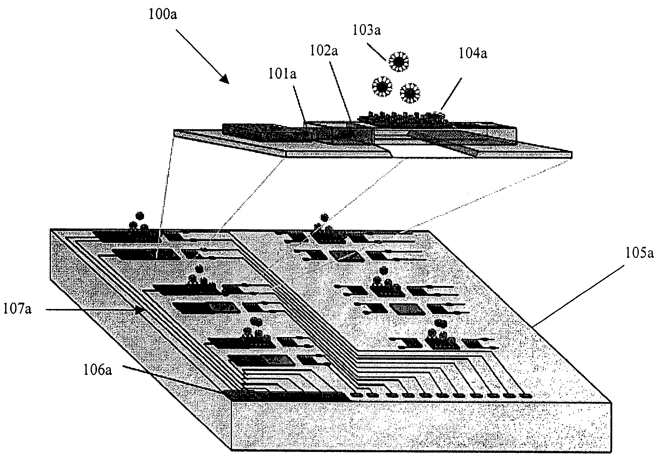
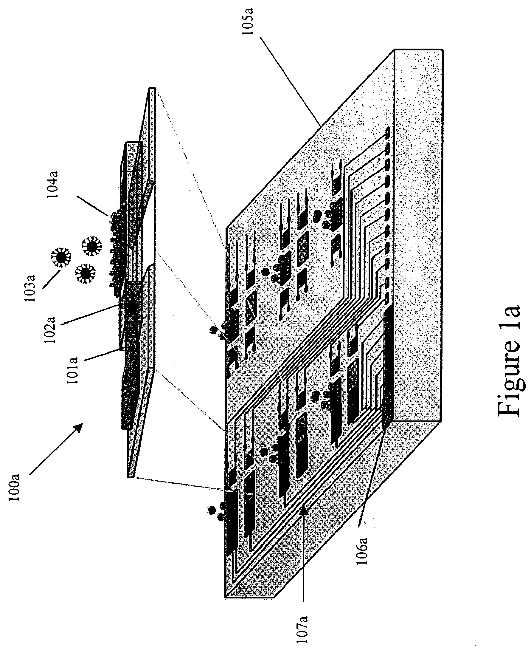
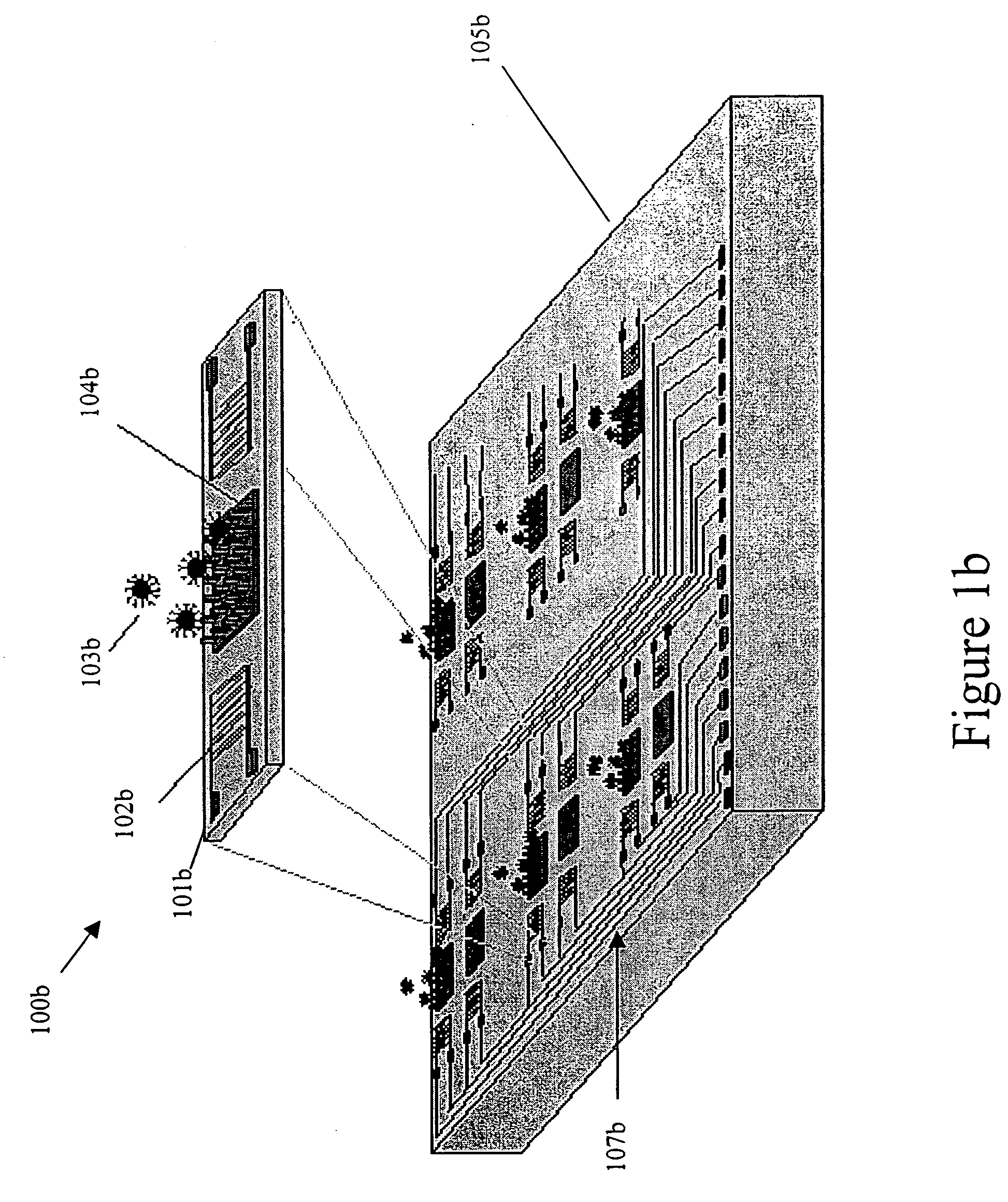
[0053]FIG. 1a shows an array arrangement of aluminum nitride-based (AlN) photo-acoustic biosensor devices integrated on a VLSI chip 105a. The array arrangement includes an integrated laser diode arrangement 106a capable of high frequency modulation, a waveguide arrangement 107a, an array of acoustic wave arrangements 100a (one is shown in expanded detail arrangement), a carbon-implanted region 102a, and a micro-machined resonating bridge 104a. An immobilization layer containing chemical and / or biological binding sites transverses the resonating bridge 104a. Interaction by an analyte 103a containing target molecules or structures binds to the resonating bridge 104a of the acoustic arrangement 100a, so as to change the resonate frequency. The change in the resonant frequency is detected by reflection using a second laser diode and a return path (such as, for example, using a waveguide) or by electronic interdigital electrodes.

[0054] During operation, the laser diode 106a pulses light...


PUM

PropertyMeasurementUnit
acoustic wavelengthaaaaaaaaaa
driving frequencyaaaaaaaaaa
frequencyaaaaaaaaaa

Abstract

An acoustic wave sensor to detect an analyte, the sensor comprising a piezoelectric material including a wide bandgap semiconductor material grown using plasma source molecular beam epitaxy.

Description

FIELD OF THE INVENTION [0001] The present invention concerns the use of acoustic wave (AW) sensors to detect chemical and biological analytes. BACKGROUND INFORMATION [0002] Acoustic wave sensors use a detection arrangement that is based on perturbations to mechanical or acoustic waves. As an acoustic wave propagates through or on the surface of the acoustive wave sensor material, any changes to the physical or chemical characteristics of the wave path may affect the velocity and / or amplitude of the acoustic wave. These changes may be correlated to the corresponding physical, chemical, or biological quantities being measured to provide sensing. [0003] Recreational inland lakes, public beaches, and parks, which may be designated for recreational purposes including fishing, swimming, etc., may be closed if there are sufficiently high levels of bacterial contamination, or other sufficiently high levels of chemical, heavy metal, and biological contaminants. At present, continuous monitor...

Claims


Application Information

Patent Timeline
Patent Type & Authority Applications(United States)
IPC IPC(8): G01H17/00G01N29/02G01N29/24G01N29/34G11B5/855H01F1/00H01L21/20H01L21/205H01L31/00
CPCB82Y10/00H01L21/02631G01N29/022G01N29/226G01N29/2418G01N29/2437G01N29/34G01N2291/0255G01N2291/0256G01N2291/0422G01N2291/0423G11B5/855H01F1/009H01L21/0242H01L21/0254B82Y25/00
Inventor AUNER, GREGORY W.ZHONG, FENGHUGHES, CHANTELLESHREVE, GINAYING, HAO
Owner AUNER GREGORY W
Why Eureka
Try Eureka