Methods of downstream microwave photoresist removal and via clean, particularly following Stop-On TiN etching

a technology of microwave photoresist and microwave etching, which is applied in the direction of photomechanical equipment, instruments, fluid pressure measurement, etc., can solve the problems of affecting the quality of the product, so as to reduce the damage and improve the product quality.

Inactive Publication Date: 2006-03-02
BELL SEMICON LLC
View PDF8 Cites 5 Cited by
  • Summary
  • Abstract
  • Description
  • Claims
  • Application Information

AI Technical Summary

Benefits of technology

[0010] Advantageously, the plasma is formed using only microwave energy, i.e., without RF energy. It has been learned that this improves product quality, at least in part by reducing plasma damage. Also advantageously, some embodiments of the present invention replace or eliminate two common steps, one being longer duration, lower temperature RIE plasma photoresist removal, and the other being solvent cleaning.
[0011] In certain embodiments, a photoresist removal method in combination with a via cleaning method follows via etching. For example, according to one embodiment of the present invention five general steps follow a Stop-On-TiN Via Etch process. These five general steps are: via sidewall clean; microwave plasma photoresist strip; cooling; cooling with temperature check, and deglazing. These steps provide for solubilizing polymer present on the via side walls to allow for subsequent water rinsing, ashing the photoresist, and removing, by deglazing, any oxide layer that may have formed in the bottom of the vias, where TiN is layered. This embodiment eliminates the need for a longer, low-temperature RIE photoresist strip step.

Problems solved by technology

However, it is recognized in the art that the use of environmentally hazardous chemicals, such as solvents used in chemical solvent cleaning, is disfavored.
Despite common use of RIE processes for photoresist stripping, it is known that the use of an RF plasma source for the RIE can lead to plasma damage.
Depending on the concentrations and energy levels of energetic atoms, radicals, ions, electrons and photons in a plasma, plasma-caused damage may include surface leakage, damage to silicon, degradation of films (especially oxides), and changes in electrical parameters.
For example, a region of high voltage plasma bombards excess ions to the wafer surface, which can result in charging of exposed metal conductors.
If the total surface area of conductors connecting to a gate is too large, the RIE plasma-induced ions striking this surface area then lead to a current discharge through the relatively thin gate oxide, which can lead to permanent damage.
While plasma damage generally is recognized to be of a greater concern during etching, where metal conductors (“antennas”) are exposed for relatively long periods compared to, for instance, plasma enhanced deposition, it has been learned that RIE plasma also is problematic in photoresist removal and via clean steps.

Method used


Image

  • Methods of downstream microwave photoresist removal and via clean, particularly following Stop-On TiN etching
  • Methods of downstream microwave photoresist removal and via clean, particularly following Stop-On TiN etching

Examples


example 1

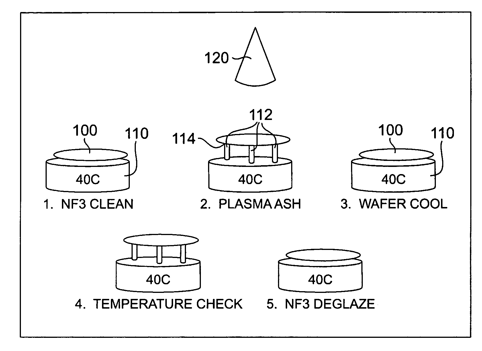
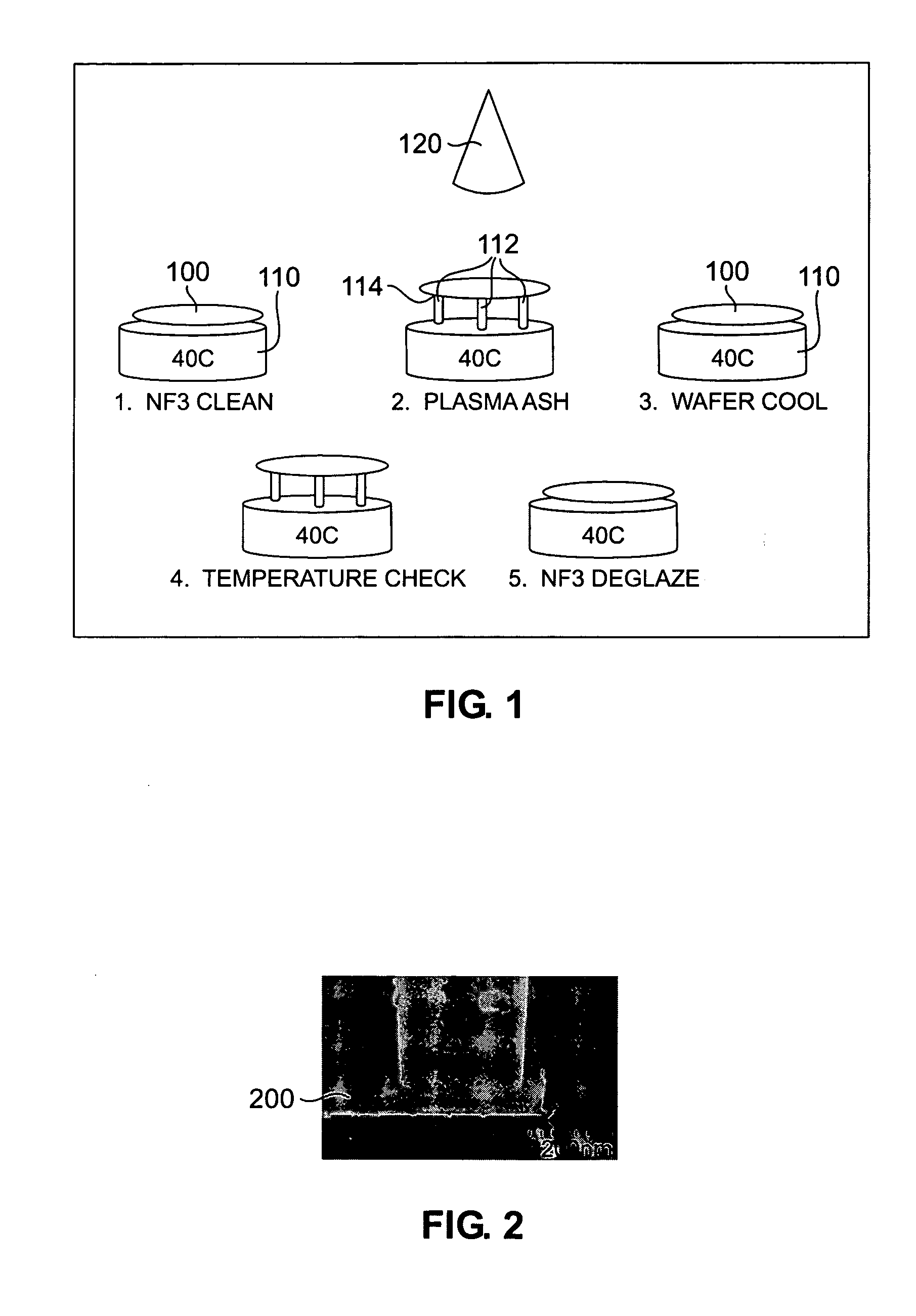
[0046] Semiconductor wafer samples undergoing fabrication were manufactured and divided into two process groups. The test circuitry includes a Metal-Oxide-Metal (MOM) capacitor between a gate pad and gate oxide. It is believed that if during a process a plasma develops a charge across the MOM capacitor, then the process has the potential to cause plasma damage at the gate oxide. If no charge is developed across the MOM capacitor, it is believed that the process would be free of effects that would cause plasma-derived damage, and the gate oxide would not be damaged during testing.

[0047] In this example, one process group used only downstream microwave plasma to strip the photoresist (i.e., via ashing) following TiN-stop etch process. This via ashing process is identified as “Via clean with downstream ash.” The other process group used downstream microwave plasma in combination with RIE plasma in the same chamber as the wafers. This group is identified as “Via clean with RIE ash.” Th...


PUM

PropertyMeasurementUnit
temperatureaaaaaaaaaa

Abstract

A process for photoresist layer removal from a semiconductor wafer comprises exposing at relatively high temperature the wafer to an RIE-free microwave-energy-generated plasma of a primary gas mixture, the exposing causing photoresist removal such as by ashing. The method also comprises determining an endpoint to the removal by a determined change in the visible light emanating from a chamber containing the wafer. A multi-step process of the present invention comprises the above method and a preliminary RIE-free microwave-energy-generated plasma that solubilizes polymer on walls of vias of the wafer. This multi-step process also comprises, following the exposing step, a cooling step, a cooling step with a temperature check, and a deglazing step. The deglazing step also uses an RIE-free microwave-energy-generated plasma. Specific gas mixtures for the respective plasmas are exemplified. Other embodiments of methods of the present invention are comprised of less steps, or a consolidation of such steps.

Description

FIELD OF INVENTION [0001] This invention relates to microwave-generated plasma methods for dry etching and dry stripping in semiconductor wafer manufacture, such as photoresist removal with via side wall polymer treatment. BACKGROUND OF THE INVENTION [0002] Numerous methods exist in semiconductor manufacture for chemical etching and for cleaning of semiconductor wafers. One category of such methods is chemical solvent cleaning. However, it is recognized in the art that the use of environmentally hazardous chemicals, such as solvents used in chemical solvent cleaning, is disfavored. Thus, methods other than chemical solvent cleaning have been developed. [0003] Key among non-solvent methods is the use of plasmas that form reactive ionized molecules that chemically etch a wafer. Plasma-based methods are used, for example, for etching and for post-process cleaning. One example of post-process cleaning is the stripping of photoresist following etching processes. Among these cleaning meth...

Claims


Application Information

Patent Timeline
Patent Type & Authority Applications(United States)
IPC IPC(8): H01L21/302B44C1/22
CPCG03F7/427H01L21/31138H01L21/31116H01L21/02063
Inventor CAMPBELL, TIMOTHY SCOTTHINCKLEY, KELLYMURPHEY, PAUL B.OMAN, DANIEL M.WHEELER, PAUL EDWARD
Owner BELL SEMICON LLC
Why Eureka
Try Eureka