Image display apparatus

a technology of image display and display screen, which is applied in the direction of discharge tube luminescnet screen, vacuum obtaining/maintenance, tubes with screens, etc., can solve the problems of affecting the display quality of images, affecting the display quality, etc., to achieve small changes in the properties of electron sources, high reliability, and small changes in the effect of electron source properties

Inactive Publication Date: 2006-03-02
CANON KK +1
View PDF2 Cites 10 Cited by
  • Summary
  • Abstract
  • Description
  • Claims
  • Application Information

AI Technical Summary

Benefits of technology

[0011] The present invention has been made in the light of the conventional problems, and an object of the present invention is to provide a method of producing an image display apparatus through a simple step, the image display apparatus showing no occurrence of leak or the like, especially, the image display apparatus showing small changes in electron source properties with time, the image display apparatus having high display quality, the image display apparatus h...

Problems solved by technology

When a gas is generated in the vacuum container to increase the pressure in the container, the increase adversely affects the electron sources to reduce an electron emission amount, thereby making it impossible to display a clear image, although the degree of the adverse effect varies depending on the kind of the gas.
In particular, the following problems are characteristic of a flat display.
The plus ion is accelerated in an electric f...

Method used


Image

  • Image display apparatus
  • Image display apparatus
  • Image display apparatus

Examples


embodiment 1

[0064] In this embodiment, an image display apparatus having a structure shown in FIG. 4, that is, an image display apparatus having an electroconductive film formed on the external surface of a rear plate was produced. The image display apparatus was provided with an electron source 105 having multiple (768 rows×3,840 columns) surface conduction electron-emitting devices wired in a simple matrix fashion on a substrate. Hereinafter, a method of producing the image display apparatus of this embodiment will be described.

[0065] Step-x1 (Production of Glass Substrate Attached With Electroconductive Film)

[0066] A glass substrate 301 of PD-200 (manufactured by Asahi Glass Co., Ltd.) having a thickness of 2.8 mm was washed with a detergent, pure water, and an organic solvent, and an ITO film having a thickness of 0.3 μm was formed on one surface of the substrate by means of ordinary sputtering. Then, the ITO film was patterned by means of ordinary photolithography to remove a high voltag...

embodiment 2

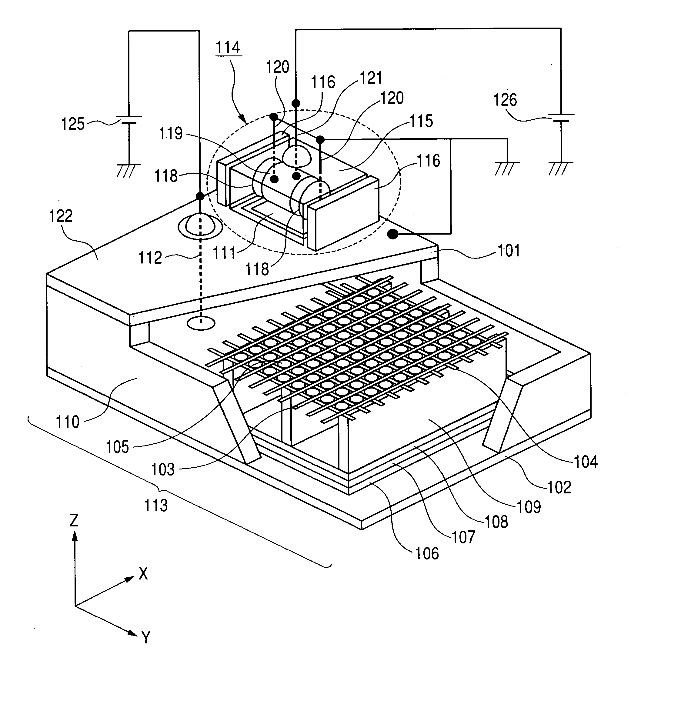
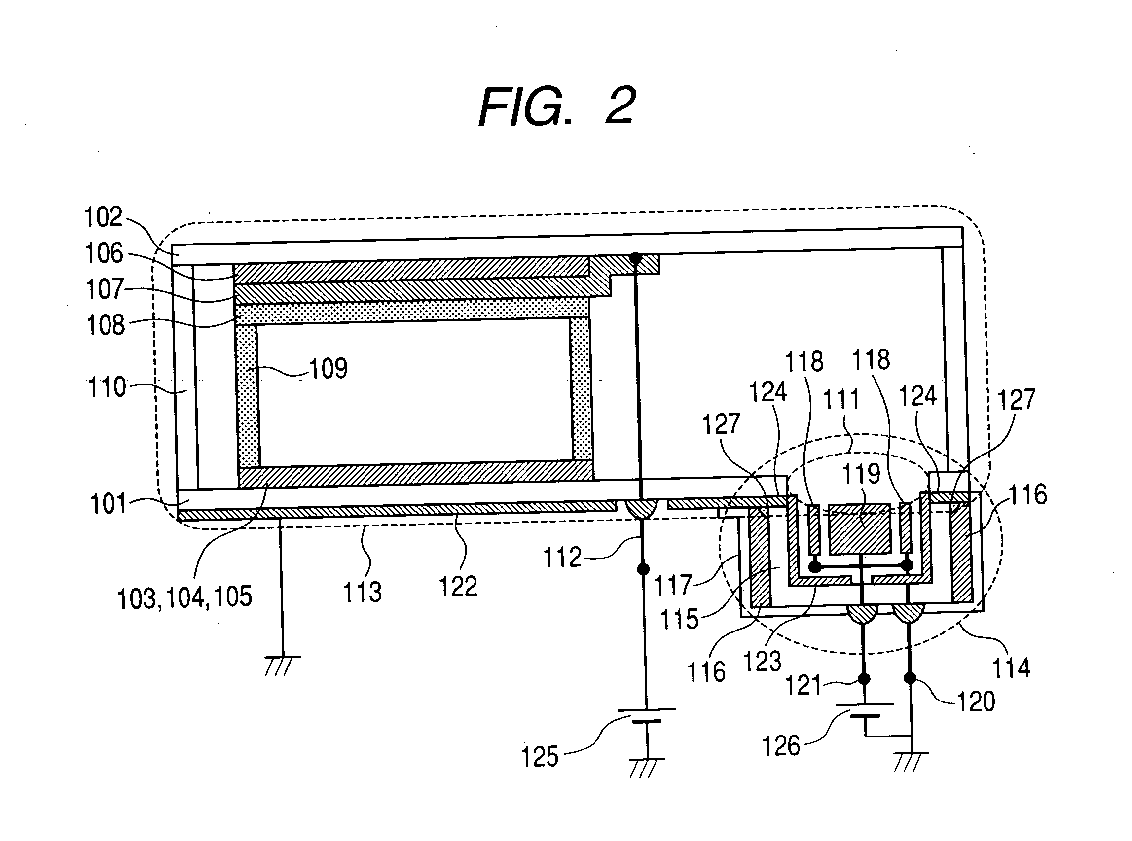
[0104] In this embodiment, an image display apparatus having a structure shown in FIG. 9, that is, an image display apparatus having an electroconductive film formed on the external surface of a rear plate and an electroconductive film formed on the internal surface of an ion pump container was produced.

[0105] Steps-x2 and a2 To g2

[0106] Steps similar to the steps-x1 and a1 to g1 described in Embodiment 1 were repeated.

[0107] Step-y2 (Assembly and Attachment of Ion Pump)

[0108] First, a glass container 115 for an ion pump perforated with holes for ion pump anode and cathode terminals was prepared. The holes may be formed by melting, or may be formed mechanically by means of a microprocessing grinding attachment. After the glass container had been washed with an organic solvent, a photoresist was applied to a predetermined position inside the glass container by means of a plate, and the whole was baked at 90° C. for 10 minutes to form a pattern for lift-off. In this state, a soluti...

embodiment 3

[0113] In this embodiment, an image display apparatus having a structure shown in FIG. 10, that is, an image display apparatus having an electroconductive film formed on the external surface of a rear plate and an electroconductive film formed on the internal surface of an ion pump container, the electroconductive film on the external surface of the rear plate being removed at a portion to be connected to an ion pump, was produced.

[0114] Step-x3 (Production of Glass Substrate Attached With Electroconductive Film)

[0115] A glass substrate 301 of PD-200 (manufactured by Asahi Glass Co., Ltd.) having a thickness of 2.8 mm was washed with a detergent, pure water, and an organic solvent, and an ITO film having a thickness of 0.3 μm was formed on one surface of the substrate by means of ordinary sputtering. Then, the ITO film was patterned by means of ordinary photolithography to remove a high voltage terminal portion and a portion to be bonded to the ion pump container in a subsequent s...


PUM


Abstract

Provided is an image display apparatus, including: a vacuum container which includes an electron source and an anode electrode opposed to the electron source; and an ion pump arranged so as to communicate through the vacuum container, in which: an ion pump container is composed of a non-electroconductive material; and an electroconductive film is formed on an external surface of the vacuum container on a side on which the ion pump container is mounted or on an internal surface of the ion pump container. The image display apparatus achieves: a reduction in weight of the ion pump; an improvement in compatibility to the vacuum container; and the prevention of an adverse effect of discharge inside the ion pump on image display.

Description

BACKGROUND OF THE INVENTION [0001] 1. Field of the Invention [0002] The present invention relates to an image display apparatus using an electron-emitting device. [0003] 2. Related Background Art [0004] In a flat display in which: a large number of electron-emitting devices are arranged as electron sources on a flat substrate; a phosphor as an image forming member on an opposing substrate is irradiated with electron beams emitted from the electron sources; and the phosphor is allowed to emit light to display an image, the inside of a vacuum container including the electron sources and the image forming member must be kept at a high vacuum. When a gas is generated in the vacuum container to increase the pressure in the container, the increase adversely affects the electron sources to reduce an electron emission amount, thereby making it impossible to display a clear image, although the degree of the adverse effect varies depending on the kind of the gas. [0005] In particular, the fol...

Claims


Application Information

Patent Timeline
IPC IPC(8): H01J27/26H01J29/94H01J31/12
CPCH01J7/14H01J7/18H01J9/385H01J2329/943H01J29/94H01J31/127H01J29/845H01J41/12H01J31/12
Inventor GOFUKU, IHACHIROKAMIO, MASARUTSUDA, HISANORISATO, YASUESHIMADA, YOSHIYUKIMITANI, HIROMASASEINO, KAZUYUKINISHIMURA
Owner CANON KK
Why Eureka
Try Eureka