Silicon oxide gapfill deposition using liquid precursors

Inactive Publication Date: 2006-03-02
APPLIED MATERIALS INC
View PDF99 Cites 19 Cited by
  • Summary
  • Abstract
  • Description
  • Claims
  • Application Information

AI Technical Summary

Benefits of technology

[0007] Embodiments of the invention provide for gapfill deposition of a silicon oxide film using a liquid Si—C—O—H precursor as a silicon source and using a gaseous oxidizer as a source of oxygen in a plasma-deposition process. A number of characteristics of the Si—C—O—H precursor provid

Problems solved by technology

One persistent challenge faced by semiconductor manufacturers in the design and fabrication of such densely packed integrated circuits is the prevention of spurious interactions between circuit elements.
High-aspect-ratio gaps are difficult to fill using conventional CVD methods, causing some integrated-circuit manufacturers to turn to the use high-density-plasma CVD (“H

Method used


Image

  • Silicon oxide gapfill deposition using liquid precursors
  • Silicon oxide gapfill deposition using liquid precursors
  • Silicon oxide gapfill deposition using liquid precursors

Examples


Embodiment Construction

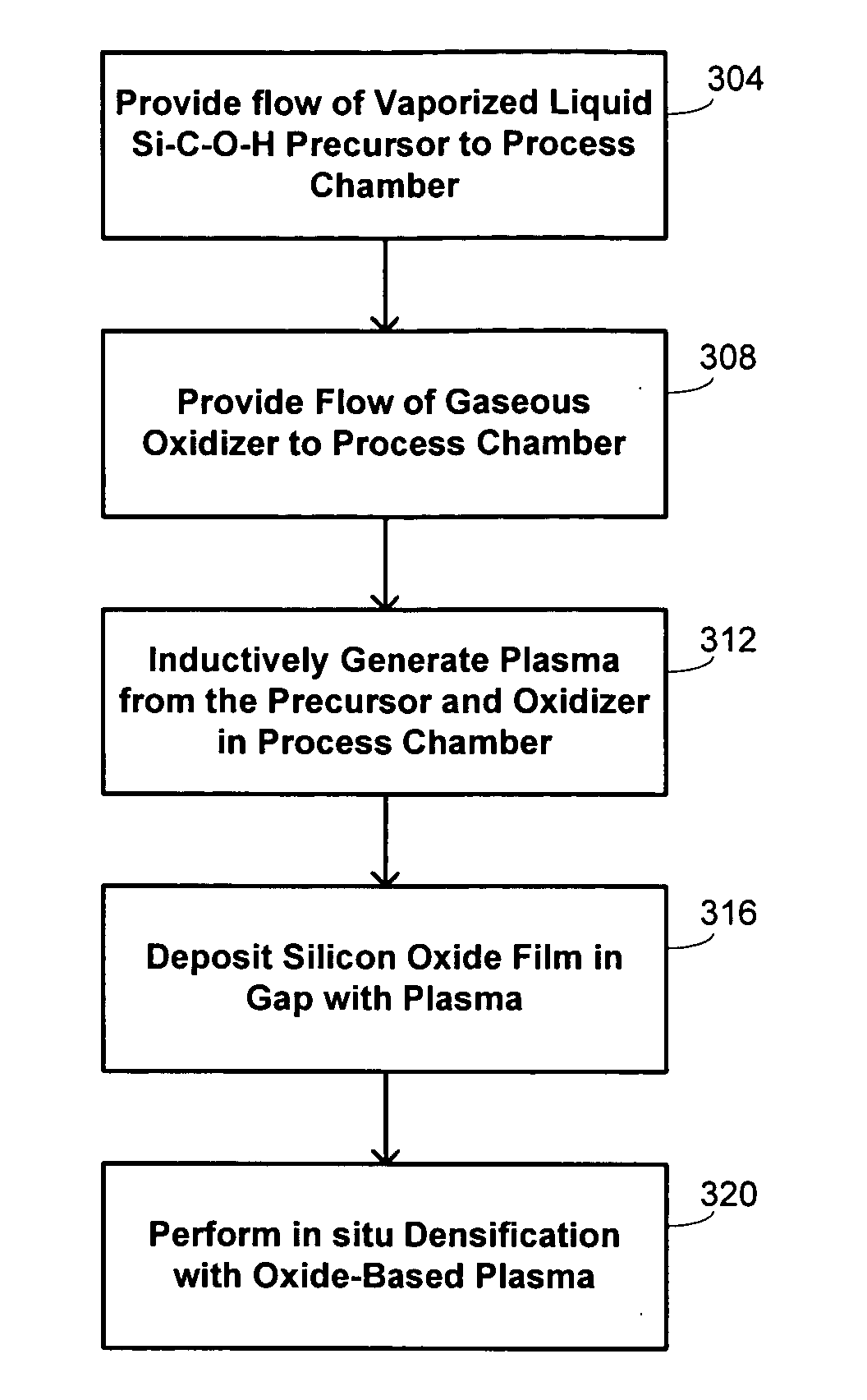
[0019] As device geometries have continued to shrink, various techniques have been developed and used in order to improve gapfill capabilities of silicon oxide deposition processes. Such techniques have tended to focus on the basic recipe of forming a high-density plasma from gaseous silane and oxygen precursors, with variations being developed in process conditions, the presence of different fluent gases, different flow rates for gases, and the like. It appears that a practical limit to achieving void-free gapfill by implementing such changes is being reached around device geometries at the scale of 50 nm and below. Embodiments of the invention use methods that deviate from the basic recipe by vaporizing a liquid Si—C—O—H precursor and forming a deposition plasma from the vaporized liquid precursor and a gaseous oxidizer, with the deposition plasma being used to fill the gap. The liquid precursors have certain physical properties that are advantageously exploited in embodiments of ...


PUM

PropertyMeasurementUnit
Temperatureaaaaaaaaaa
Nanoscale particle sizeaaaaaaaaaa
Dielectric polarization enthalpyaaaaaaaaaa

Abstract

A silicon oxide film is deposited on a substrate disposed in a substrate processing chamber. The substrate has a gap formed between adjacent raised surfaces. A liquid Si—C—O—H precursor is vaporized. A flow of the vaporized liquid Si—C—O—H precursor is provided to the substrate processing chamber. A gaseous oxidizer is also flowed to the substrate processing chamber. A deposition plasma is generated inductively from the precursor and the oxidizer in the substrate processing chamber, and the silicon oxide film is deposited over the substrate and within the gap with the deposition plasma.

Description

BACKGROUND OF THE INVENTION [0001] One common step that may be performed frequently during fabrication of modem semiconductor devices is the formation of a film, such as a silicon oxide film, on a semiconductor substrate. Silicon oxide is widely used as an insulating film in the manufacture of semiconductor devices and, as is well known, may be deposited as a film by a thermal chemical vapor deposition (“CVD”) process or by a plasma-enhanced CVD (“PECVD”) process. In conventional thermal CVD processes, reactive gases are supplied to the substrate surface, where heat-induced chemical reactions take place to form the desired film. In a conventional plasma process, a controlled plasma is formed to decompose and / or energize reactive species to produce the desired film. [0002] Semiconductor-device geometries have decreased significantly in size since such devices were originally developed several decades ago. This decrease in device-geometry size has consequently resulted in an increase ...

Claims


Application Information

Patent Timeline
IPC IPC(8): H01L21/31
CPCC23C16/401H01L21/02164H01L21/0234H01L21/02274H01L21/02214
Inventor NEMANI, SRINIVAS D.LEE, YOUNG S.
Owner APPLIED MATERIALS INC
Why Eureka
Try Eureka