

Hierarchical method of power supply noise and signal integrity analysis
a power supply and signal integrity analysis technology, applied in error detection/correction, program control, instruments, etc., can solve the problems of significant erroneous at the higher frequencies commonly used today, improper assessment of signal integrity, and difficulty in accurately modeling these electrical phenomena, so as to reduce the number of elements, improve computational efficiency, and accurately simulate
- Summary
- Abstract
- Description
- Claims
- Application Information
AI Technical Summary
Benefits of technology
Problems solved by technology
Method used
Image

Examples
Embodiment Construction
[0045] Although certain embodiments of the present invention will be shown and described in detail, it should be understood that various changes and modifications may be made without departing from the scope of the appended claims. The scope of the present invention will in no way be limited to the number of constituting components, the materials thereof, the shapes thereof, the relative arrangement thereof, etc., and are disclosed simply as an example of an embodiment. The features and advantages of the present invention are illustrated in detail in the accompanying drawings, wherein like reference numerals refer to like elements throughout the drawings.
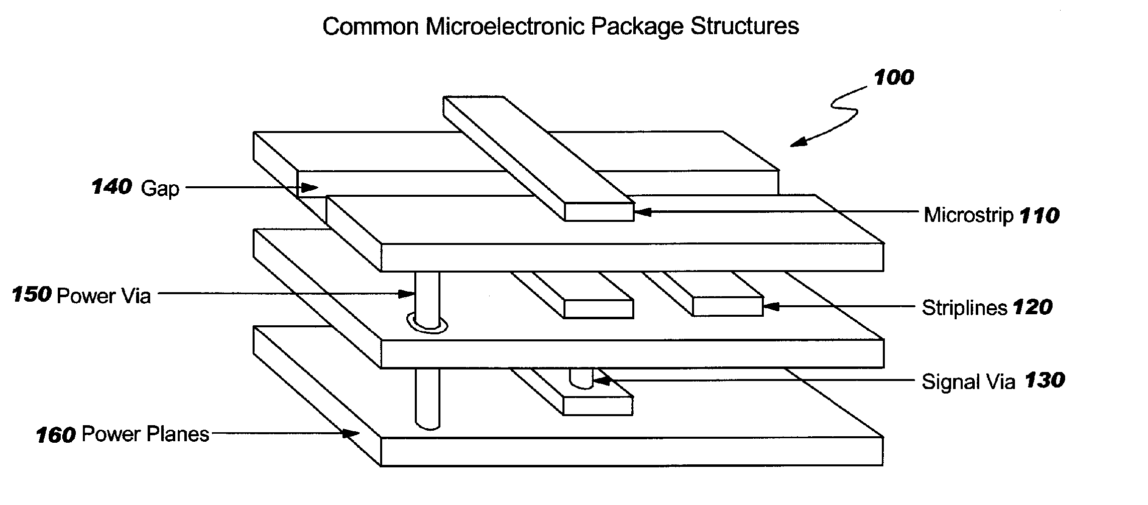
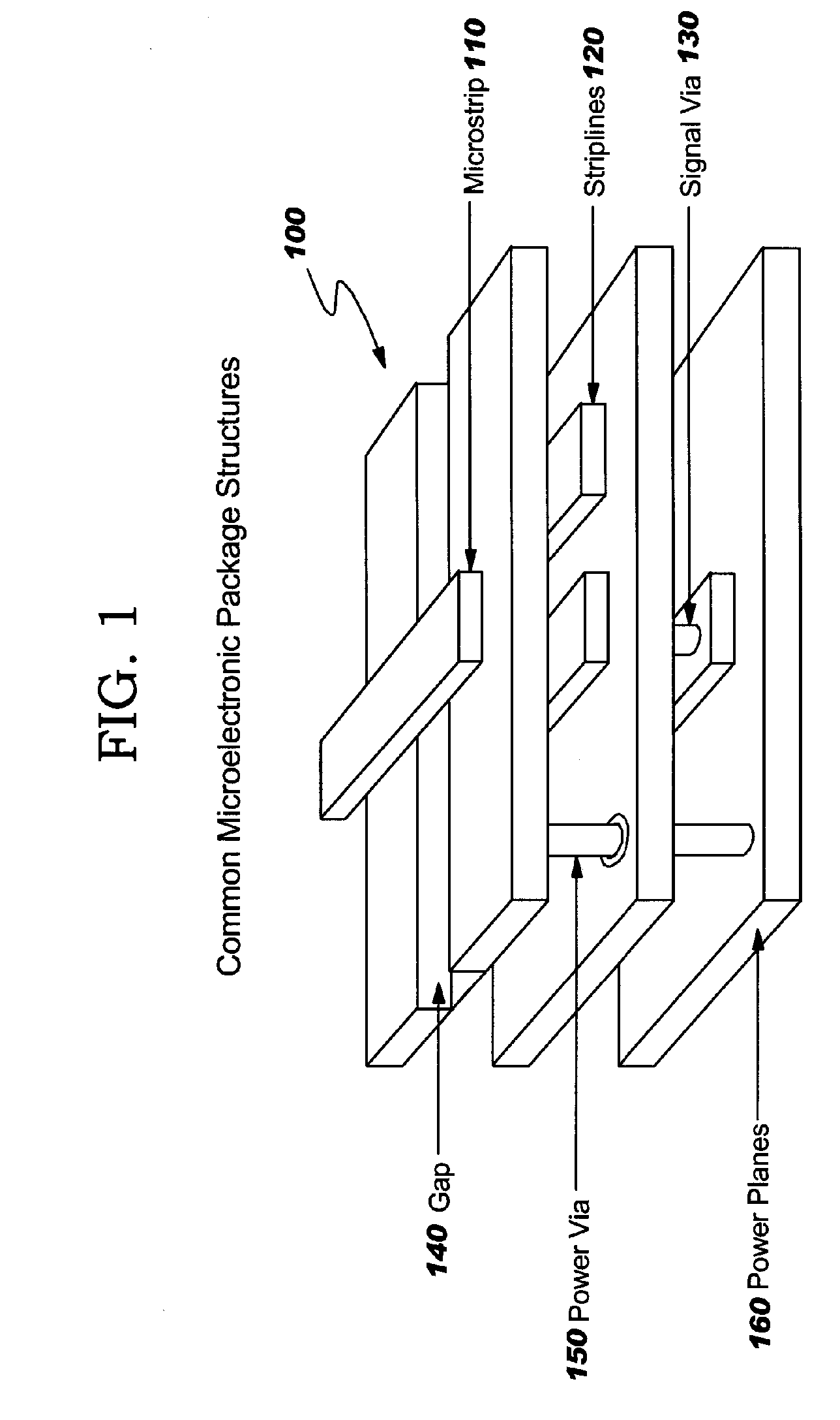
[0046] The invention described herein provides a method of creating a frequency-dependent electrical model of any electrical system which has a structure that can be modeled as an orthogonal geometric structure. One such electrical system is an integrated chip package which contains horizontal wires, vertical vias, and horizontal c...
PUM
 Abstract
Description
Claims
Application Information