Non-volatile memory cells employing a transition metal oxide layer as a data storage material layer and methods of manufacturing the same

a technology of transition metal oxide and data storage material, which is applied in the field of semiconductor devices, can solve the problems of difficult to form a uniform composition pcmo layer on the semiconductor substrate, difficulty in patterning the pcmo layer using a conventional photolithography/etching process, and difficulty in improving the integration density of resistance ram devices

Active Publication Date: 2006-03-16
SAMSUNG ELECTRONICS CO LTD
View PDF7 Cites 193 Cited by
  • Summary
  • Abstract
  • Description
  • Claims
  • Application Information

AI Technical Summary

Problems solved by technology

However, it is difficult to pattern the PCMO layer using a conventional photolithography / etch process, which is widely used in the fabrication of semiconductor devices.
This patterning complexity may lead to difficulties in improvement of integration density of resistance RAM devices employing a PCMO layer.
Thus, it may be difficult to form the PCMO layer having a uniform composition throughout the semiconductor substrate.

Method used


Image

  • Non-volatile memory cells employing a transition metal oxide layer as a data storage material layer and methods of manufacturing the same
  • Non-volatile memory cells employing a transition metal oxide layer as a data storage material layer and methods of manufacturing the same
  • Non-volatile memory cells employing a transition metal oxide layer as a data storage material layer and methods of manufacturing the same

Examples


Embodiment Construction

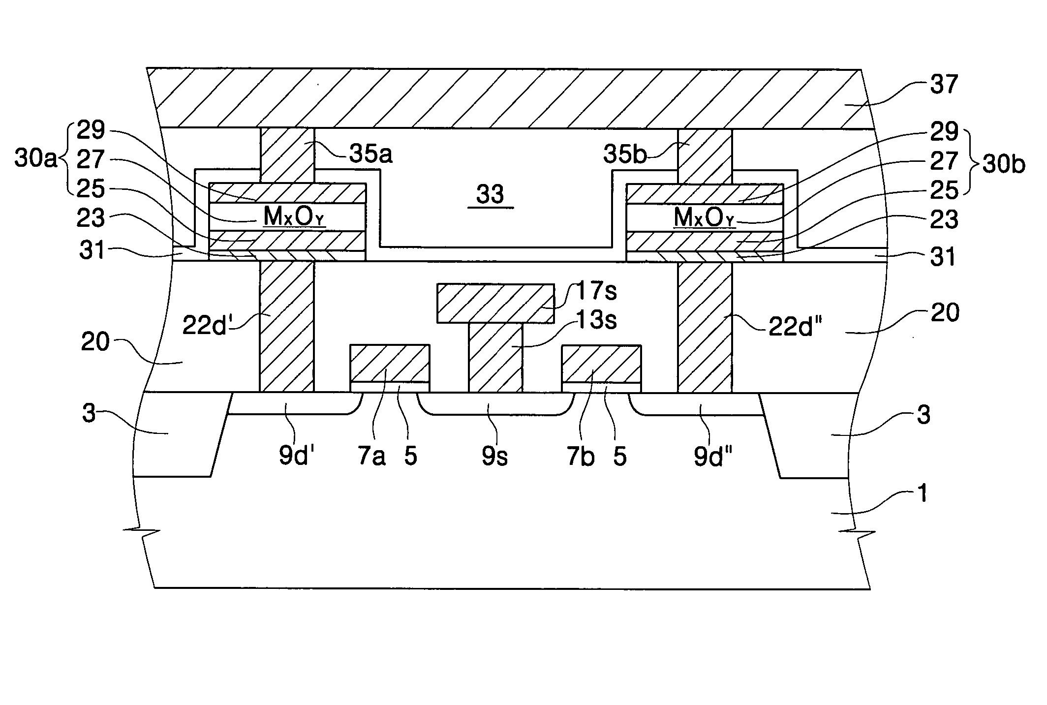
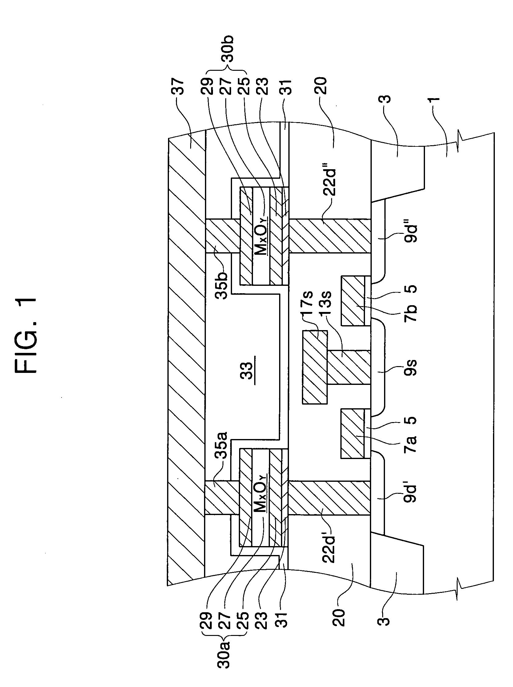
[0024] The present invention will now be described more fully with reference to the accompanying drawings, in which exemplary embodiments of the invention are shown. The invention may, however, be embodied in many different forms and should not be construed as being limited to the embodiments set forth herein; rather, these embodiments are provided so that this disclosure will be thorough and complete, and will fully convey the concept of the invention to those skilled in the art. In the drawings, the thicknesses of layers and regions are exaggerated for clarity. Like reference numerals in the drawings denote like elements.

[0025]FIG. 1 is a cross-sectional view illustrating a pair of non-volatile memory cells, e.g., a pair of resistance RAM cells according to embodiments of present invention. Referring to FIG. 1, an isolation layer 3 is provided at a predetermined region of a semiconductor substrate 1 to define an active region. First and second drain regions 9d′ and 9d″, which are...


PUM


Abstract

Non-volatile memory cells employing a transition metal oxide layer as a data storage material layer are provided. The non-volatile memory cells include a lower and upper electrodes overlapped with each other. A transition metal oxide layer pattern is provided between the lower and upper electrodes. The transition metal oxide layer pattern is represented by a chemical formula MxOy. In the chemical formula, the characters “M”, “O”, “x” and “y” indicate transition metal, oxygen, a transitional metal composition and an oxygen composition, respectively. The transition metal oxide layer pattern has excessive transition metal content in comparison to a stabilized transition metal oxide layer pattern. Methods of fabricating the non-volatile memory cells are also provided.

Description

CROSS-REFERENCE TO RELATED APPLICATION [0001] This application claims the priority of Korean Patent Application No. 2004-72754, filed Sep. 10, 2004, the disclosure of which is hereby incorporated herein in its entirety by reference. FIELD OF THE INVENTION [0002] The present invention relates to semiconductor devices and methods of manufacturing the same and, more particularly, to non-volatile memory devices and methods of manufacturing non-volatile memory devices. BACKGROUND OF THE INVENTION [0003] Non-volatile memory devices retain their stored data even when their power supplies are turned off. Therefore, non-volatile memory devices have been widely used in computers, mobile teleconmmunication systems, memory cards and so on. Flash memory devices are widely used as non-volatile memory devices. Many flash memory devices employ memory cells having a stacked gate structure. The stacked gate structure includes a tunnel oxide layer, a floating gate, an inter-gate dielectric layer and a...

Claims


Application Information

Patent Timeline
Patent Type & Authority Applications(United States)
IPC IPC(8): H01L29/94
CPCH01L27/112H01L27/115H01L45/1608H01L27/2436H01L45/04H01L45/1233H01L45/146H01L45/1253H10B63/30H10N70/20H10N70/826H10N70/841H10N70/8833H10N70/021H10B20/00H10B69/00
Inventor BAEK, IN-GYULEE, MOON-SOOK
Owner SAMSUNG ELECTRONICS CO LTD
Why Eureka
Try Eureka