Solid state imaging device, method of manufacturing same, and digital camera

a solid-state imaging and manufacturing method technology, applied in the direction of radioation control devices, television systems, television system scanning details, etc., can solve the problems of reducing sensitivity, difficult to detect the corresponding signal, and incomplete transfer of charge, so as to suppress cracks and the like, and improve the hydrogen supply capacity

Inactive Publication Date: 2006-03-23
CANON KK
View PDF8 Cites 90 Cited by
  • Summary
  • Abstract
  • Description
  • Claims
  • Application Information

AI Technical Summary

Benefits of technology

[0012] The present invention has been made to solve the above-mentioned problems, and therefore has an object to provide a hydrogen supply structure suitable for a MOS type solid state imaging device. Another object of the present invention is to provide a solid state imaging device with...

Problems solved by technology

At this point, when a lattice defect exists on an interface of an oxide film under a gate of the transfer transistor, the charge generated in the photodiode is trapped by the defect, causing an incomplete transfer of the charge.
Thus, in a state in which such a defect exists, and particularly in the case where a small amount of light is to be detected, it is hard to detect the corresponding signal.
Therefore, the above-described defect causes a lowering of sensitivity, and becomes a cause for generating a dark current or noise.
Further, a defect due to a dangling bond on the interface of the oxide film is dominant over various kinds of defects as a defect that generates a carrier trap.
However, when the thickness of the surface protection film increases, an internal stress in the film increases accordingly.
As a result, a damaged portion such as a crack tends to occur.
Further, it is considered that an expansion or tensile stress is applied to the film depending on the temperature of heat treatment after the formation ...

Method used


Image

  • Solid state imaging device, method of manufacturing same, and digital camera
  • Solid state imaging device, method of manufacturing same, and digital camera
  • Solid state imaging device, method of manufacturing same, and digital camera

Examples


first embodiment

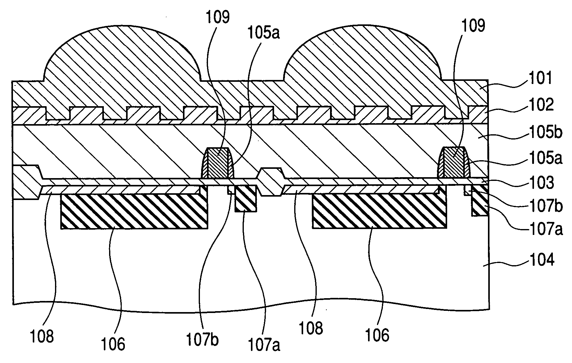
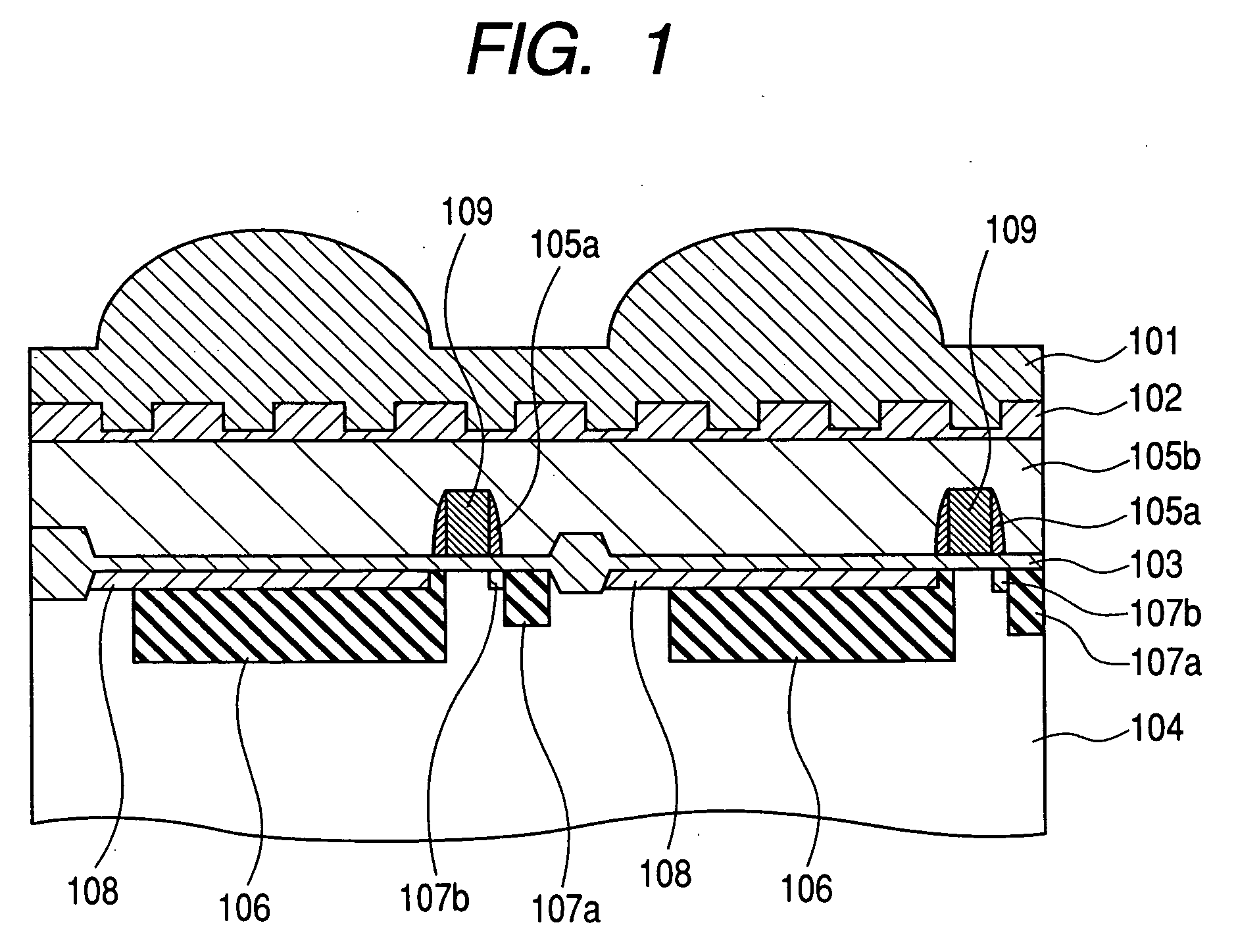
[0034] Hereinafter, description will be made of a first embodiment with reference to FIG. 1. FIG. 1 is a sectional view of a portion corresponding to two pixels in a solid state imaging device in accordance with the first embodiment of the present invention.

[0035] In the solid state imaging device, an n-type semiconductor region capable of storing signal charge (n-type storage region) 106 is formed in a p-type well 104 formed on a surface of a semiconductor substrate made of silicon. A surface p-type semiconductor region 108 with a high impurity concentration, which is electrically connected with the p-type well 104, is formed on the n-type storage region 106. These components form an embedded photodiode functioning as a light receiving element that generates signal charge. Note that the light receiving element is not limited to an embedded type one, but is preferably of the embedded type for attaining, for example, reduction of surface defects.

[0036] Further, an oxide film 103 is...

second embodiment

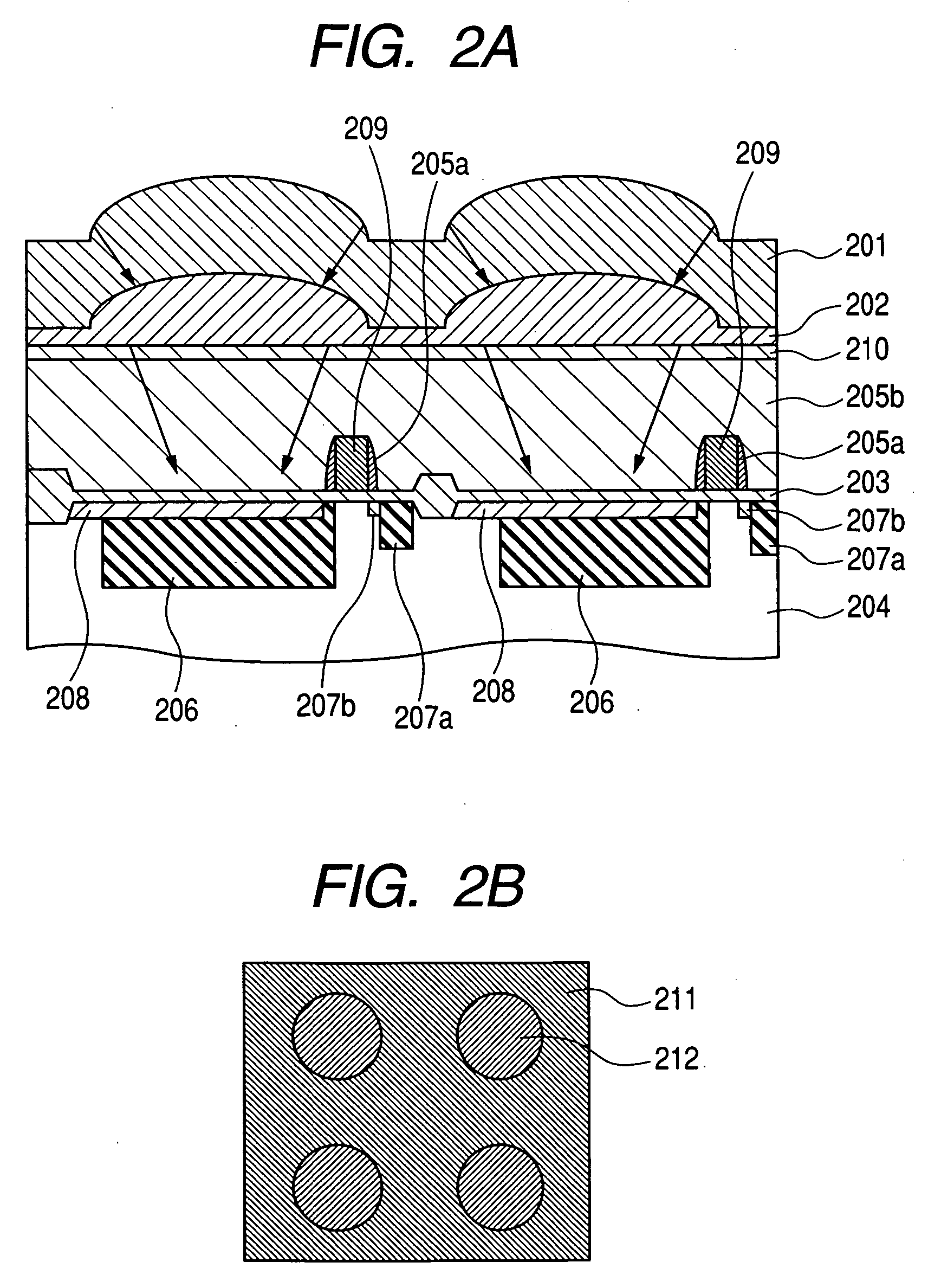
[0044] Description will be made of a second Embodiment with reference to FIGS. 2A and 2B. FIG. 2A is a sectional view, and FIG. 2B is a plan view.

[0045] A structure of a light receiving element is the same as in the first embodiment, and thus, detailed description thereof will be omitted. Moreover, in the second Embodiment, an embedded photodiode that is a light receiving element is constituted by an n-type storage region 206, which is formed in a p-type well 204 disposed on a surface of a semiconductor substrate, and according to a surface p-type semiconductor region 208 with a high impurity concentration.

[0046] Further, reference numeral 203 denotes an oxide film formed through thermal oxidation, and reference numeral 209 denotes a transfer electrode 209 made of polycrystalline silicon. Formed on both sides of the transfer electrode 209 are side wall films 205a each of which is composed of a residual silicon oxide film at the time of etching-back of a silicon oxide film. With th...

third embodiment

[0052] Description will be made of a third embodiment with reference to FIGS. 3A and 3B. FIG. 3A is a sectional view, and FIG. 3B is a plan view. Also in the second embodiment, an embedded photodiode functioning as a light receiving element is constituted by an n-type storage region 306, which is formed in a p-type well 304 formed on a surface of a semiconductor substrate made of silicon, and a surface p-type semiconductor region 308 with a high impurity concentration which is electrically connected with the p-type well 304. Further, a transfer electrode 309 made of polycrystalline silicon is formed on an oxide film 303 formed on the semiconductor substrate through thermal oxidation. Formed on both sides of the transfer electrode 309 are side wall films 305a each of which is made of a residual silicon oxide film at the time of etching-back of a silicon oxide film. Therefore, an LDD structure can be provided.

[0053] In the third embodiment, a silicon nitride oxide film 310, which con...


PUM


Abstract

Provided is a MOS type solid state imaging device, including a semiconductor substrate, a plurality of pixels arranged on the semiconductor substrate, each pixel having a light receiving element for generating a signal charge due to incident light, and a MOS transistor for reading the signal charge, and a hydrogen supply film arranged on the semiconductor substrate over the plurality of pixels and having a region corresponding to the light receiving element at least a part of which has a film thickness greater than the other part of the region.

Description

BACKGROUND OF THE INVENTION [0001] 1. Field of the Invention [0002] The present invention relates to a solid state imaging device, a method of manufacturing the solid state imaging device, and a digital camera that utilizes the solid state imaging device, and particularly relates to a solid state imaging device that includes an amplification element for each pixel or for each group of plural pixels. [0003] 2. Related Background Art [0004] Currently, a photodiode is generally used as a light receiving element that converts an optical signal into an electric signal through light absorption. An active sensor (APS: Active Pixel Sensor), which amplifies a charge subjected to photoelectric conversion with the photodiode by means of an amplification element provided per pixel (or plural pixels) to generate a detection signal, is commercially available as a solid state imaging device provided in, for example, a digital camera. [0005] In such a sensor, the charge generated in the photodiode ...

Claims


Application Information

Patent Timeline
IPC IPC(8): H04N5/335H01L27/14H01L27/146
CPCH01L27/14621H01L27/14625H01L31/0232H01L27/1463H01L27/14627H01L31/02327
Inventor IIDA, SATOKOWATANABE, TAKANORI
Owner CANON KK
Why Eureka
Try Eureka