Method of fabricating dual damascene interconnections of microelectronic device using diffusion barrier layer against base material

a technology of diffusion barrier layer and microelectronic device, which is applied in the manufacturing of semiconductor/solid-state devices, basic electric elements, electric devices, etc., can solve the problems of photoresist poisoning, degrading electrical properties of the lower interconnection, and reducing the depth of focus margin, so as to achieve the effect of improving properties and/or performan

Active Publication Date: 2006-03-23
SAMSUNG ELECTRONICS CO LTD
View PDF16 Cites 35 Cited by
  • Summary
  • Abstract
  • Description
  • Claims
  • Application Information

AI Technical Summary

Benefits of technology

[0009] To solve some or all of the above-described problems, it is an object of the present invention to pro...

Problems solved by technology

When the via is not filled with a filler, the via may create a step height at a photoresist layer coated for forming a trench, resulting in a reduction in the depth of focus (DOF) margin; also, an etch stop layer may be etched during etching and cleaning steps thereby exposing a lower interconnection,...

Method used


Image

  • Method of fabricating dual damascene interconnections of microelectronic device using diffusion barrier layer against base material
  • Method of fabricating dual damascene interconnections of microelectronic device using diffusion barrier layer against base material
  • Method of fabricating dual damascene interconnections of microelectronic device using diffusion barrier layer against base material

Examples


experimental example 1

[0065] After a CVD OSG (k=2.9) as an ILD was formed on a substrate to a thickness of 7,000 Å, a via was formed, and some base materials (N:) such as nitrogen or amine remained within the ILD as the result of an ashing process using nitrogen-based plasma. Subsequently, after an HSQ-based material (in the above formula (1), R is octadecyl, x is 0.24, and y is 0.76) was formed on the CVD OSG to a thickness of 2,000 Å, photoresist for ArF was formed thereon. Then, a photoresist pattern defining a trench was formed after going through exposure using exposure light having a wavelength of 193 nm and development using a tetramethylammonium hydroxide developing solution, thereby preparing a first test sample in accordance with the present invention.

[0066] After a CVD OSG (k=2.9) as an ILD was formed on a substrate to a thickness of 7,000 Å, some base materials (N:) such as nitrogen or amine remained within the ILD as the result of a nitrogen-based plasma process. Subsequently, after MSQ was...

experimental example 2

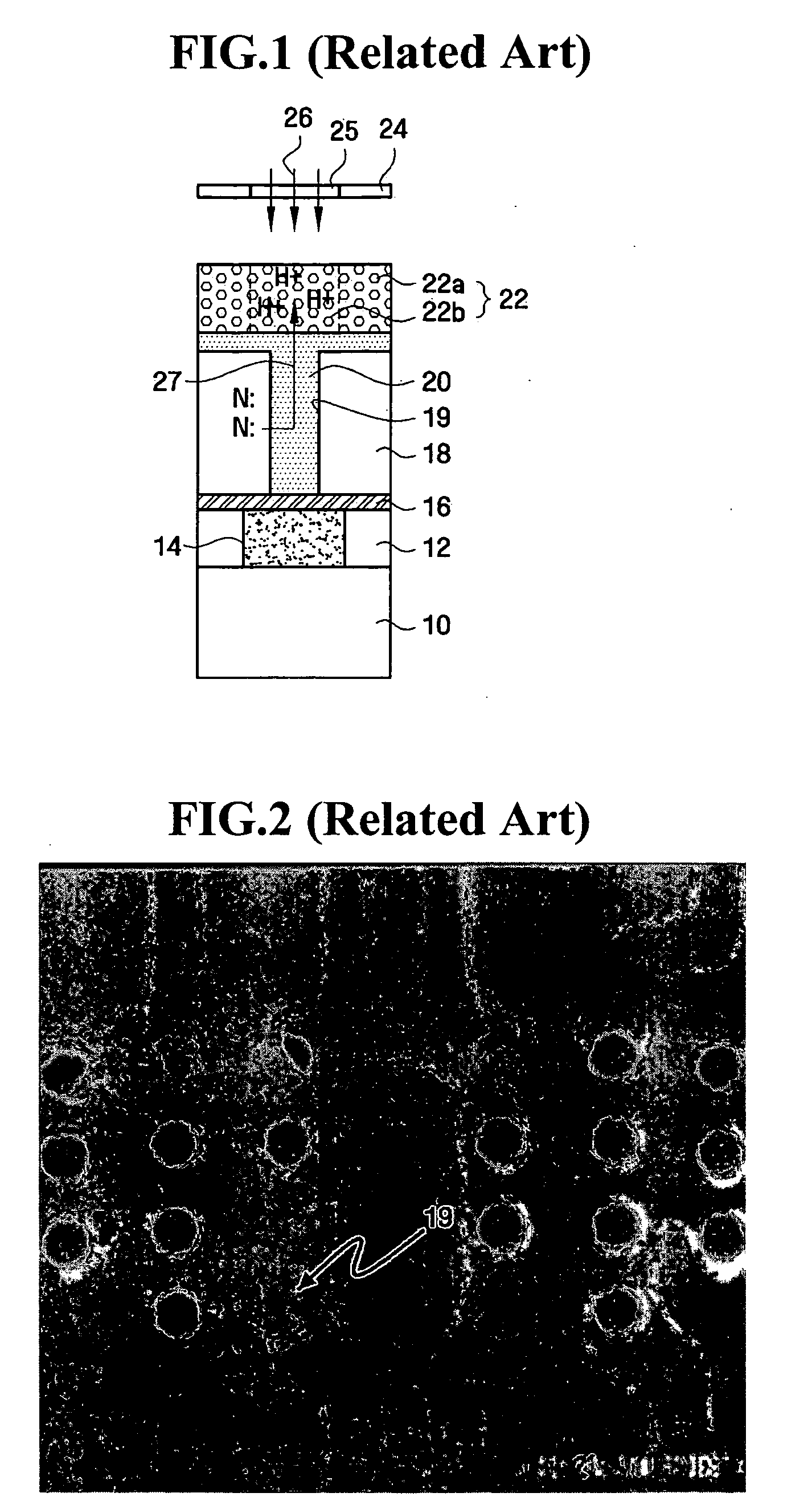
[0068] The first embodiment of the present invention was applied to fabricating a logic device having dual damascene interconnections of a 90 nm-design-rule logic device with embedded 1.1 μm2 6Tr-SRAM. Thus, a photoresist pattern defining a trench with dual damascene interconnections according to the present invention was formed. SEM imaging of the resultant structure is shown in FIG. 24. It can be seen that the formed photoresist pattern had no observable damage, which represents a significant improvement over the prior art.

[0069] According to a method of fabricating dual damascene interconnections according to one embodiment of the present invention, an ILD is formed of a hybrid low-k material and a via filler may be formed of an HSQ-based material having a diffusion barrier characteristic to protect against base materials and also having an anti-reflecting function. As a result, photoresist poisoning is suppressed, an etch stop layer protecting a lower interconnection is not dam...


PUM


Abstract

Methods of fabricating dual damascene interconnections suitable for use in microelectronic devices and similar applications using a diffusion barrier layer to protect against base materials during processing are provided. The methods include the steps of: filling a via with a hydrogen silsesquioxane (HSQ)-based filler as expressed by the general chemical formula: (RSiO3/2)x(HSiO3/2)y, wherein x and y satisfy the relationships x+y=1 and 0<x<y<1, and R is selected from C4-C24 alkyl, C4-C24 alkenyl, C4-C24 alkoxy, C8-C24 alkenoxy, substituted C4-C24 hydrocarbon, non-substituted C1-C4 hydrocarbon or substituted C1-C4 hydrocarbon; and, partially etching the filler filling the via and an interlayer dielectric to form a trench, which is connected to the via in the region where the dual damascene interconnections are to be formed. Then, the filler remaining in the via is removed, and the trench and the via are filled with an interconnection material to complete the dual damascene interconnections.

Description

[0001] This application claims priority from Korean Patent Application No. 2004-061163 filed on Aug. 3, 2004 in the Korean Intellectual Property Office, the disclosure of which is incorporated herein by reference in its entirety. BACKGROUND OF THE INVENTION [0002] 1. Field of the Invention [0003] The present invention relates to a method of fabricating a microelectronic device, and more particularly, to a method of fabricating dual damascene interconnections for use in or with a microelectronic device. [0004] 2. Description of the Related Art [0005] As microelectronic devices have become more efficient and highly integrated, multi-layered interconnections are more widely used in fabricating such devices. To obtain a reliable device including multi-layered interconnections, each interconnection layer is preferably formed in a planar fashion. To achieve such a planar configuration, dual damascene interconnections have become a familiar fabrication technique. [0006] Among methods of fa...

Claims


Application Information

Patent Timeline
IPC IPC(8): H01L21/4763H01L21/31
CPCH01L21/3124H01L21/76826H01L21/76808H01L21/02134H01L21/28
Inventor LEE, KYOUNG-WOOMAENG, JAE-YEOLKIM, JAE-HAKOH, IL-WHANSHIN, HONG-JAE
Owner SAMSUNG ELECTRONICS CO LTD
Why Eureka
Try Eureka