Dual-gate thin-film transistor

Inactive Publication Date: 2006-03-30
SHARP LAB OF AMERICA
View PDF16 Cites 22 Cited by
  • Summary
  • Abstract
  • Description
  • Claims
  • Application Information

AI Technical Summary

Benefits of technology

[0008] The present invention describes the fabrication of a dual-gate TFT having two controlling “gates”, a top gate and a back (bottom) gate. One unique feature of this device is the extension of the bottom gate beyond the contacts to the S/D electrodes of the device, to alleviate

Problems solved by technology

If the bottom gate is larger than the top gate and has vertical sidewalls, then undoped regions are formed in the active channel adjacent the back gate sides, which are undesira

Method used


Image

  • Dual-gate thin-film transistor
  • Dual-gate thin-film transistor
  • Dual-gate thin-film transistor

Examples


Example

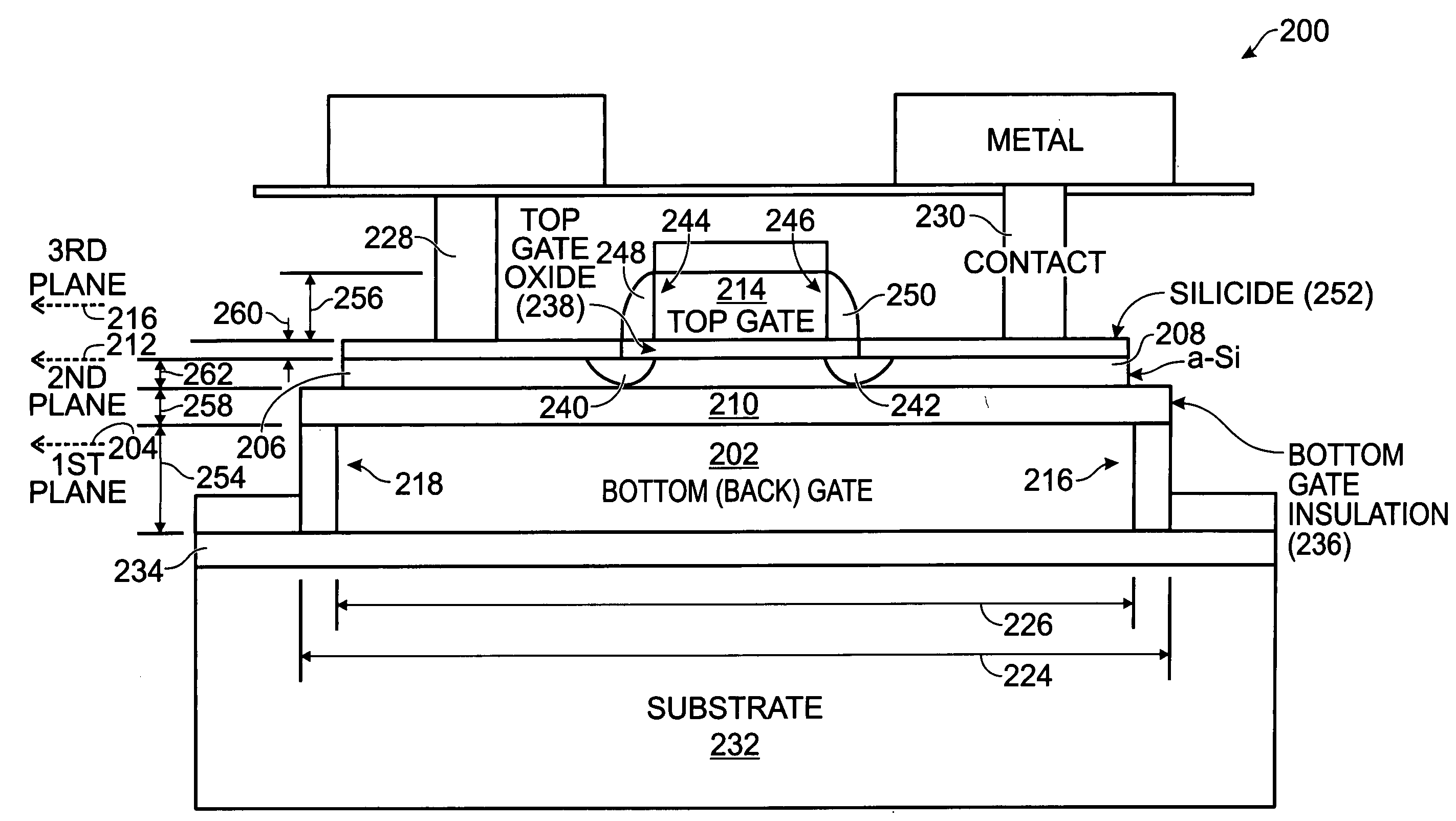
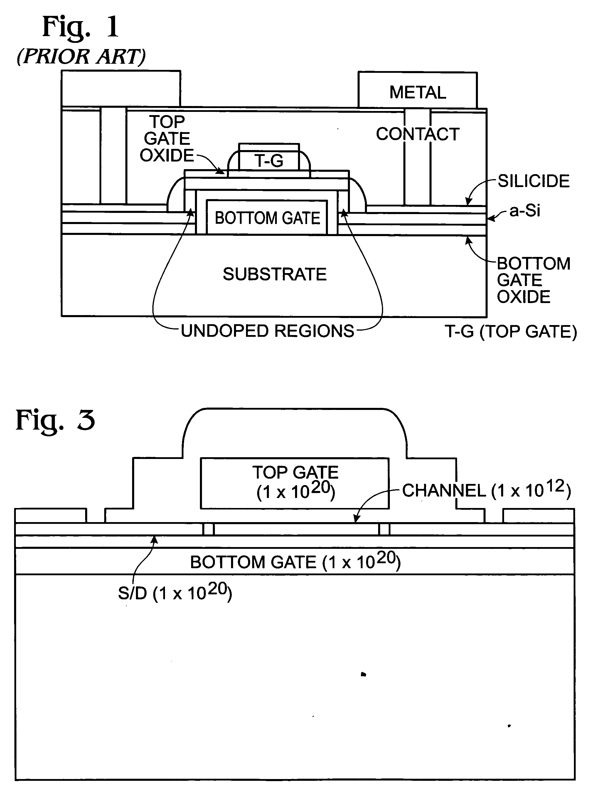
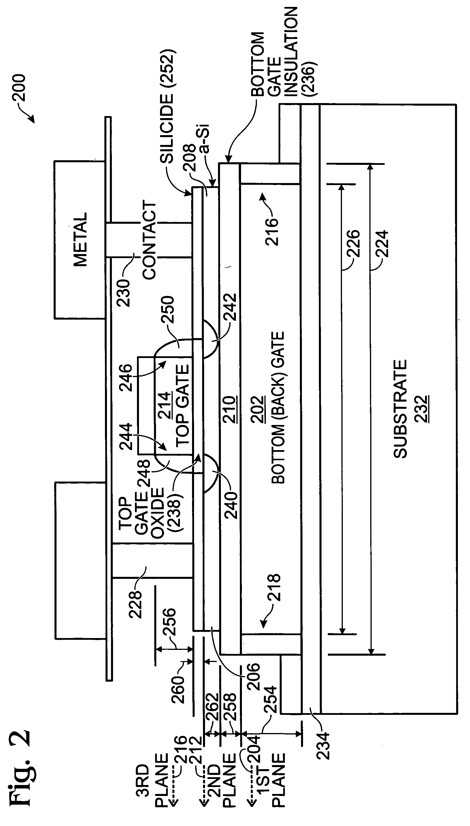
[0020]FIG. 2 is a partial cross-sectional view of the present invention dual-gate thin film transistor (DG-TFT). The DG-TFT 200 comprises a first (back) gate 202 aligned in a first horizontal plane 204. A first polycrystalline silicon (poly-Si) source / drain (S / D) region 206, a second poly-Si S / D region 208, and an intervening poly-Si channel region 210 are aligned in a second horizontal plane 212, overlying the first plane 204. A second gate 214 is aligned in a third horizontal plane 216, overlying the second plane 212.

[0021] The definition of the element's respective horizontal planes is somewhat arbitrary. The element positions can be defined with respect to a top surface, bottom surface, or by approximate mid-height. As shown, the elements 202, 206, 208, 210, and 212 are defined as their mid-heights being in a specified plane. However, their positions can alternately be defined by top or bottom surfaces. Note, the term “horizontal” is used herein as a convenient visual reference...


PUM


Abstract

A dual-gate thin film transistor (DG-TFT) and associated fabrication method are provided. The method comprises: forming a first (back) gate in a first horizontal plane; forming source/drain (S/D) regions and an intervening channel region in a second horizontal plane, overlying the first plane; and, forming a second (top) gate in a third horizontal plane, overlying the second plane. The S/D regions and intervening channel region have a combined length, smaller than the length of the first gate. A substrate insulating layer is formed over the substrate, made from a material such as SiO2. A first gate insulation layer is formed over the first gate. Amorphous silicon (a-Si) is deposited over the first gate insulation layer and crystallized. The S/D and channel regions are formed from the crystallized Si layer. A second gate oxide layer is formed over the channel region.

Description

BACKGROUND OF THE INVENTION [0001] 1. Field of the Invention [0002] This invention generally relates to integrated circuit (IC) and liquid crystal display (LCD) fabrication and, more particularly, to a dual-gate thin-film transistor DG-TFT, with the source, drain, and intervening channel regions for a top gate, directly overlying a bottom gate. [0003] 2. Description of the Related Art [0004] There are several fabrication processes that can be manipulated to influence the characteristics of a transistor. One of the most important transistor properties is threshold voltage or Vt, which is a measure of the field at which a device begins to conduct. Vt affects the speed and power consumption of CMOS devices with higher speed and higher power at lower Vt and low speed / power for high Vt. Thus, it is useful to be able to vary the Vt of a transistor for programmable power circuits, and it is useful to tune Vt to compensate for variations in the fabrication process. Typically, Vt is a set pr...

Claims


Application Information

Patent Timeline
IPC IPC(8): H01L21/84
CPCG09G3/20G09G3/3208H01L29/78648G09G2300/08G09G2310/0262G09G3/3659
Inventor SCHUELE, PAUL J.VOUTSAS, APOSTOLOS T.
Owner SHARP LAB OF AMERICA
Why Eureka
Try Eureka