Conductive pad design modification for better wafer-pad contact

a technology of conductive pads and design modifications, which is applied in the direction of grinding machine components, manufacturing tools, lapping machines, etc., can solve the problems of excessive conditioning, non-planar feature side of the substrate, and needing planarization

Inactive Publication Date: 2006-04-06
APPLIED MATERIALS INC
View PDF99 Cites 34 Cited by
  • Summary
  • Abstract
  • Description
  • Claims
  • Application Information

AI Technical Summary

Problems solved by technology

As layers of materials are sequentially deposited and removed, the feature side of the substrate may become non-planar and require planarization.
Inherent in this challenge is the difficulty in producing a pad that will not react with process chemistry, which may cause degradation, or require excessive conditioning.
This upper surface may not sufficiently contact the feature side of the substrate, possibly leaving regions of the feature side without sufficient or stable electrical bias.
This regional or intermittent bias may adversely affect the polishing process.

Method used


Image

  • Conductive pad design modification for better wafer-pad contact
  • Conductive pad design modification for better wafer-pad contact
  • Conductive pad design modification for better wafer-pad contact

Examples


Embodiment Construction

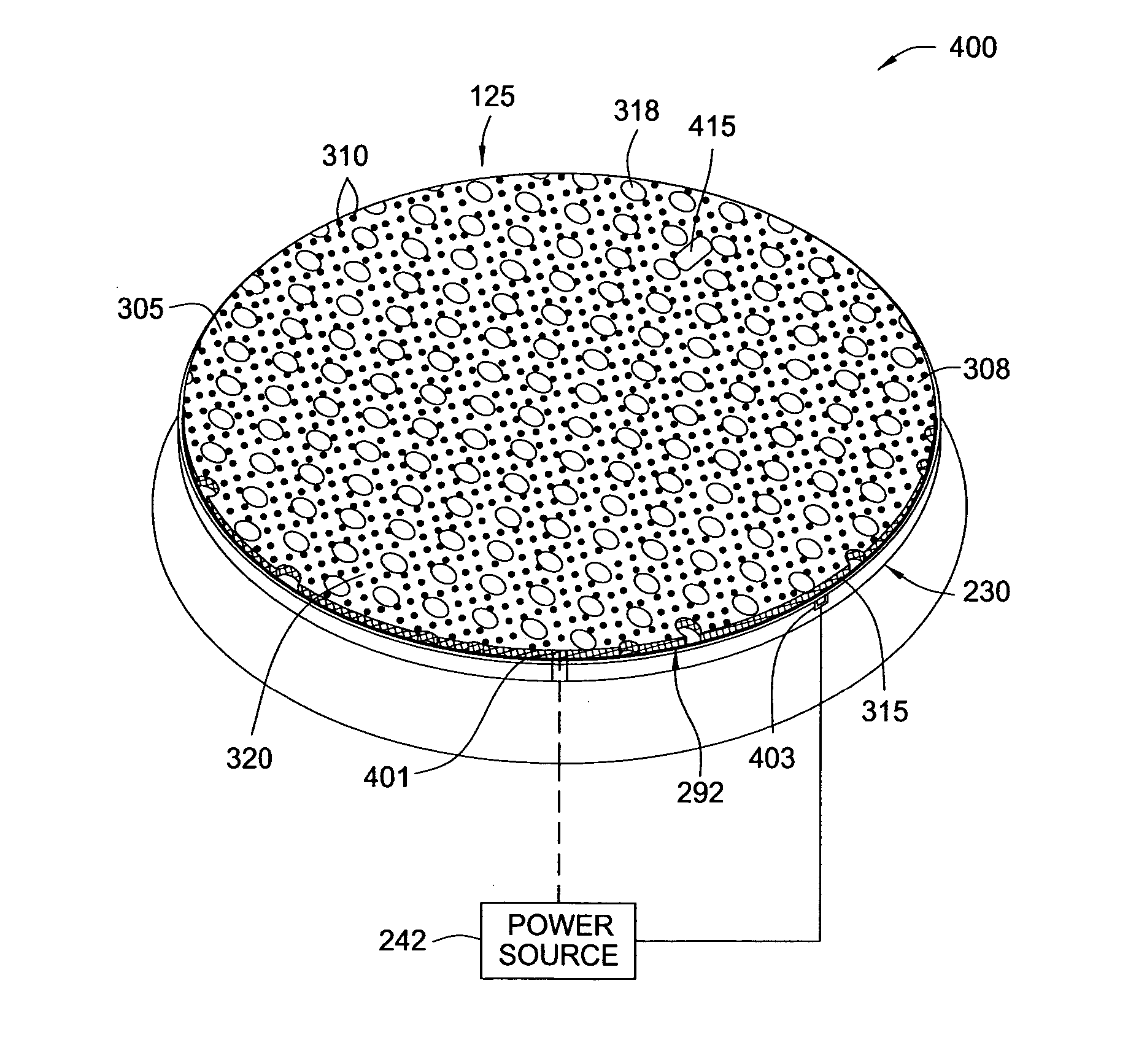
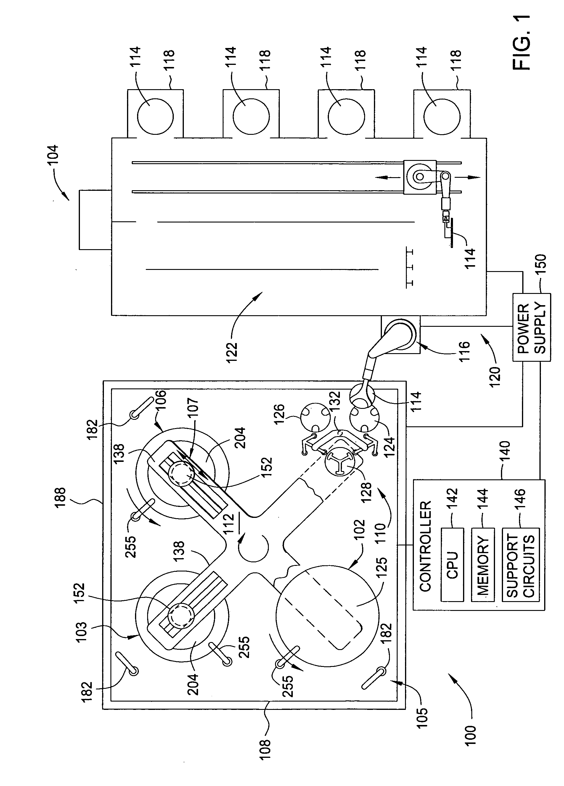
[0023]FIG. 1 depicts a processing apparatus 100 having a planarizing module 105 that is suitable for electrochemical mechanical polishing and chemical mechanical polishing. The planarizing module 105 includes at least one electrochemical mechanical planarization (ECMP) station 102, and optionally, at least one conventional chemical mechanical planarization (CMP) station 106 disposed in an environmentally controlled enclosure 188. Examples of planarizing modules 105 that may be adapted to benefit from the invention include MIRRA®, MIRRA MESA™, REFLEXION®, REFLEXION LK®, REFLEXION LK Ecmp™ Chemical Mechanical Planarizing Systems, all available from Applied Materials, Inc. located in Santa Clara, Calif. Other planarizing modules commonly used in the art may also be adapted to benefit from the invention.

[0024] For example, in the planarizing module 105 shown in FIG. 1, the apparatus includes a first ECMP station 102, a second ECMP station 103, and one CMP station 106. The stations may ...


PUM

PropertyMeasurementUnit
sizeaaaaaaaaaa
lengthaaaaaaaaaa
lengthaaaaaaaaaa

Abstract

An apparatus and method for manufacturing and refurbishing a conductive polishing pad assembly for performing an electrochemical process on a substrate is disclosed. The conductive polishing pad assembly is formed using a contact surface as a foundation that is coated with a metallic coating to create a conductive contact surface. In one embodiment, the metallic coating is a high purity tin/zinc alloy that is sprayed on the contact surface. The contact surface contains abrasive particles while the metallic coating provides at least conductive qualities to the contact surface.

Description

CROSS-REFERENCE TO RELATED APPLICATIONS [0001] This application claims benefit of U.S. provisional patent application Ser. No. 60 / 616,028, filed Oct. 5, 2004, which is herein incorporated by reference.BACKGROUND OF THE INVENTION [0002] 1. Field of the Invention [0003] Embodiments of the present invention generally relate to a processing apparatus for planarizing or polishing a substrate. More particularly, the invention relates to polishing pad design for planarizing or polishing a semiconductor wafer by electrochemical mechanical planarization. [0004] 2. Description of the Related Art [0005] In the fabrication of integrated circuits and other electronic devices on substrates, multiple layers of conductive, semiconductive, and dielectric materials are deposited on or removed from a feature side, i.e., a deposit receiving surface, of a substrate. As layers of materials are sequentially deposited and removed, the feature side of the substrate may become non-planar and require planariz...

Claims


Application Information

Patent Timeline
Patent Type & Authority Applications(United States)
IPC IPC(8): B24B49/00B24B37/04B24B37/22B24B37/24
CPCB23H5/08B24B37/046B24B37/22B24B37/245H01L21/32125
Inventor MAVLIEV, RASHID A.KARUPPIAH, LAKSHMANAN
Owner APPLIED MATERIALS INC
Why Eureka
Try Eureka