Low-k dielectric functional imprinting materials

a dielectric functional and imprinting technology, applied in the direction of photosensitive materials, instruments, photomechanical equipment, etc., can solve the problems of difficult selection or selection of organic materials, significant challenges in the development of appropriate organic polymers, and the complexity of patterning processes, so as to improve the release of cured compositions

Inactive Publication Date: 2006-04-20
MOLECULAR IMPRINTS
View PDF99 Cites 78 Cited by
  • Summary
  • Abstract
  • Description
  • Claims
  • Application Information

AI Technical Summary

Benefits of technology

[0013] As the UV curing is preferably conducted through a mold that is UV transparent, another object of achieving a robust process for imprinting includes using a UV curable polymerizab

Problems solved by technology

However, the development of appropriate organic polymers, as well as their depositions and patterning methods poses significant challenges.
The selection or choice of an organic material is frequently limited by the need for higher temperature steps in other aspects of the process, such as metallization or semiconductor fabrication.
Although porous inorganic materials can inherently withstand higher processing temperatures, like other dielectri

Method used


Image

  • Low-k dielectric functional imprinting materials
  • Low-k dielectric functional imprinting materials
  • Low-k dielectric functional imprinting materials

Examples


example 1

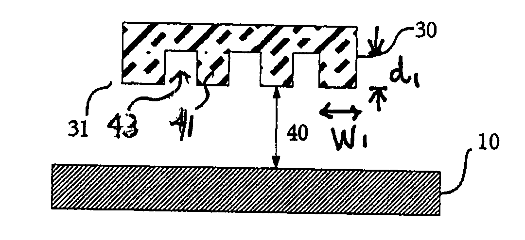
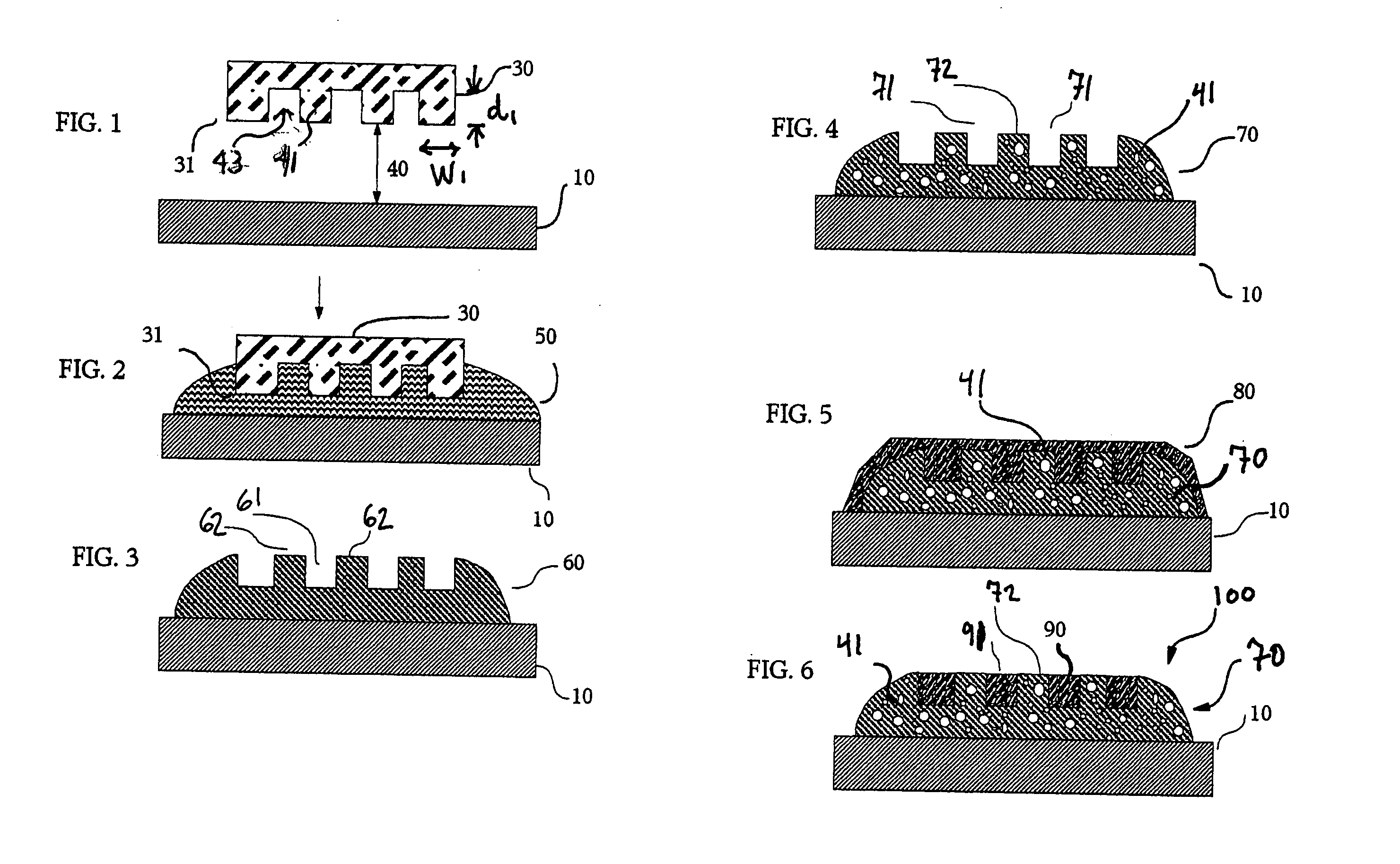
[0049] As a theoretical example of a preferred composition for the polymerizable fluid of the instant invention, 79.5 g ORMOCER b59 UV curable organic modified silicate, 20 g TONE 0301 as the porogen and 0.5 g FC4432 of fluorosurfactant are mixed together. As ORMOCER b59 is available from the manufacturer premixed with the appropriate photo initiator the above composition can be used for imprint molding as described above when exposed to UV radiation of a wavelength that includes 365 nm. “TONE” 0310 is a poly(caprolactone) polyol (CAS Reg. No. 37625-56-2) having a relatively low-melting point and is tri-functional (3 —OH groups per molecule) with a number average molecular weight of about 900, and a hydroxyl number (mg KOH / g) of 187.0, being available from the Dow Chemical Company (Midland, Mich.). Other polycaprolactones deemed suitable without undue experimentation include CAPA 3031, which is available from Solvay Caprolactones (Warrington, Cheshire, United Kingdom).
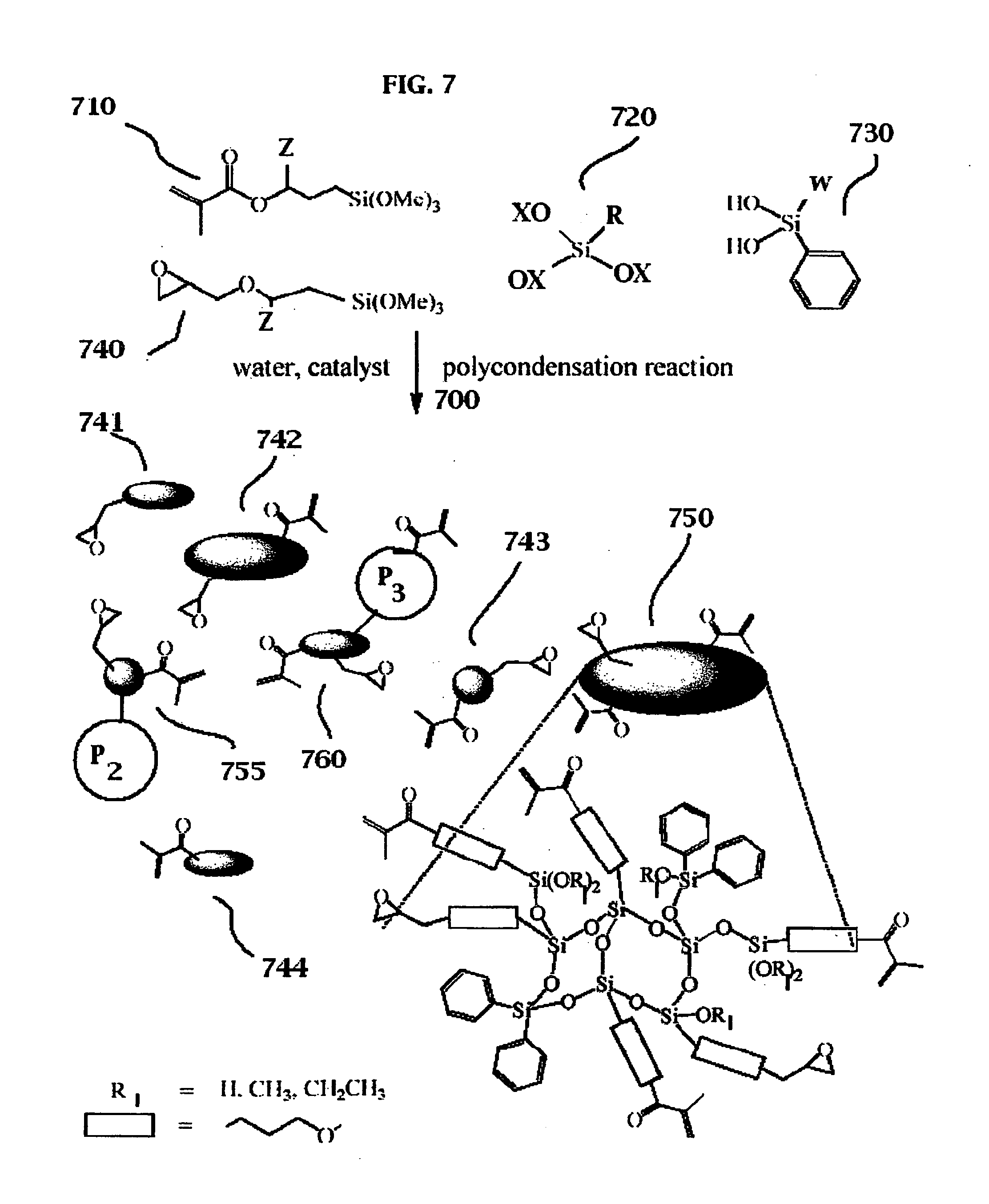
[0050] It is ...


PUM

PropertyMeasurementUnit
Percent by massaaaaaaaaaa
Massaaaaaaaaaa

Abstract

In a substantially planar circuit, the conductors are separated by an inorganic material with a dielectric constant of less than about 3.0. The dielectric layers are formed in a process that includes defining trenches and/or vias for the conductors by imprinting an initially planar layer of a radiation curable composition. The imprinting die is preferably UV transparent such that the composition is UV cured while the imprint die is in place. The curable composition includes an organic modified silicate compound and a second decomposable organic component, the latter forming nanometer scale pores as the organic compounds are subsequently decomposed to provide a polysilicate matrix. The pores reduce the effective dielectric constant from that of otherwise dense silicon dioxide.

Description

BACKGROUND OF INVENTION [0001] The present invention relates to a method or material of fabricating integrated circuits, and in particular to a method of forming an integrated circuit on a substrate having a low dielectric constant. [0002] There is a continuing desire in the microelectronics industry to increase the circuit density in multilevel integrated circuit devices, e.g., memory and logic chips, thereby increasing their performance and reducing their cost. In order to accomplish this goal, it is also desirable to reduce the minimum feature size on the chip, e.g., circuit line width, and also to decrease the dielectric constant of the interposed dielectric material to enable closer spacing of circuit lines without an increase in crosstalk and capacitive coupling. Further, there is a desire to reduce the dielectric constant of the dielectric materials such as utilized in the back end of the line (BEOL) portion of integrated circuit devices, which contain input / output circuitry,...

Claims


Application Information

Patent Timeline
IPC IPC(8): C03C15/00G03C1/492
CPCB82Y10/00B82Y40/00G03F7/0002Y10T428/24612H01L21/7682Y10T428/24545H01L21/76817H01L2221/1047B81C1/0046
Inventor XU, FRANK Y.CHUN, JUN SUNGWATTS, MICHAEL P. C.
Owner MOLECULAR IMPRINTS
Why Eureka
Try Eureka