Light emitting device having circuit protection unit

a light emitting device and protection unit technology, applied in the direction of lasers, basic electric elements, semiconductor lasers, etc., can solve the problems of high manufacturing cost, complex packaging process and insufficient protection of light emitting devices by circuit protection units, so as to prevent or mitigate excess forward current, reduce manufacturing complexity and cost, and prevent electrostatic damage

Inactive Publication Date: 2006-04-20
EPISTAR CORP
View PDF7 Cites 71 Cited by
  • Summary
  • Abstract
  • Description
  • Claims
  • Application Information

AI Technical Summary

Benefits of technology

[0011] Due to the above-mentioned combinations of a low-resistance layer with a potential barrier layer, the forward threshold voltage of the circuit protection unit is high and the reverse breakdown voltage of the circuit protection unit is low. The circuit protection unit with rectification function is integrated in the light emitting device such that the damage resulted from an electrostatic discharge or excessive forward current is prevented or mitigated effectively.
[0012] Specifically, the forward bias voltage and breakdown voltage of the circuit protection unit are Vsf and Vsr respectively. The forward operating voltage, forward damage voltage, and breakdown voltage of light emitting device are Vf, Vfd, and Vr respectively, wherein Vf<|Vsf|<Vfd, |Vsr|<|Vr|. When the light emitting device is driven by the forward operating voltage Vf and the forward operating voltage Vf<|Vsf|, the circuit protection unit is turned off. When the light emitting device is driven by a forward operating voltage higher than Vfd, the circuit protection unit is turned on because of |Vsf|<Vfd. As a result, the excessive forward current is prevented from passing through and damaging the light emitting device, and the light emitting device is protected by the circuit protection unit. On the other hand, when the light emitting device is driven by a reverse operating voltage, the circuit protection unit is turned on (the reverse operating voltage=Vsr) before the reverse operating voltage reaches Vr because of |Vsr|<|Vr|. As a result, the excessive reverse current is prevented from passing through and damaging the light emitting device, and the light emitting device is still protected by the circuit protection unit.
[0013] Additionally, the circuit protection unit of the present invention is manufactured by a conventional chip manufacturing process. There is no need to bond a Zener diode or a shunt diode with the light emitting diode during the packaging process. Besides, the light emitting diode having the circuit protection unit of the present invention can be a flip chip type light emitting device such that the Zener diode can be omitted to reduce manufacturing complexity and cost.
[0014] Furthermore, the light emitting diode of the present invention has a circuit protection unit for preventing the electrostatic damage during manufacturing. As a result, the stringent requirements for environmental to reduce electrostatic discharge is relaxed. In addition, the yield rate for light emitting diodes is greatly improved.
[0015] The present invention describes a light emitting device having a circuit protection unit. The light emitting device includes a light emitting stacking layer having a first surface and a second surface and the circuit protection unit. Furthermore, the circuit protection unit includes a low-resistance layer and a potential barrier layer, wherein a barrier potential exists at the interface between the low-resistance layer and the potential barrier layer. The circuit protection uni forms an electrical connection with each of the first surface and the second surface of the light emitting stacking layer, thus accomplishing a rectifying function.

Problems solved by technology

However, the circuit protection unit is electrically connected with the light emitting device during the packaging process, i.e., the light emitting device is not protected by the circuit protection unit before the packaging process.
Specifically, the light emitting device is not protected by the circuit protection unit adequately during the chip manufacturing process of the light emitting device.
Moreover, the light emitting device packaging process described above is complex and the manufacturing cost is high.
Because the light emitting diode chip is soldered with the shunt diode after dicing, the damage caused by electrostatic discharge during the manufacturing of the light emitting diode is still unavoidable.
Furthermore, the manufacturing process requires an additional procedure for soldering the light emitting diode with the shunt diode, thus incurring a relatively high cost.
Therefore, the reverse current may pass through the light emitting diode directly and the light emitting diode is damaged when the reverse current becomes excessive.

Method used


Image

  • Light emitting device having circuit protection unit
  • Light emitting device having circuit protection unit
  • Light emitting device having circuit protection unit

Examples


third embodiment

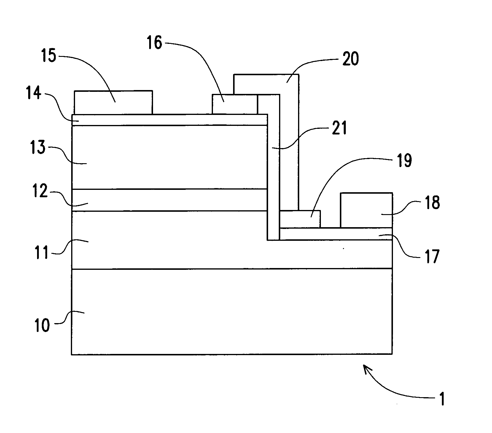
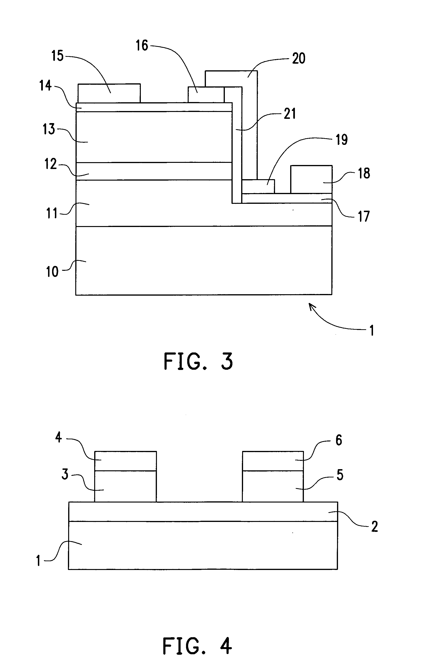
[0044] Referring to FIG. 7, the third light emitting device 3 having circuit protection unit, in accordance with the present invention, is illustrated. It should be noted that identical numericals represent the same elements in FIGS. 3FIG. 7. Therefore, description related to these elements is omitted here. In the light emitting device 3 as shown in FIG. 7, a bonding layer 310 is provided between the substrate 10 and the first stacking layer 11. The first stacking layer 11 is adhered onto the substrate 10 by wafer bonding technology.

[0045] In another embodiment of the present invention, the substrate 10 and the first stacking layer 11 are bonded directly under rising temperature and pressure without using the bonding layer 301. After the substrate 10 and the first stacking layer 11 are bonded directly under rising temperature and pressure, the first electrode and second electrode is disposed on opposite sides of the light emitting device. The layout of the circuit protection unit is...

fourth embodiment

[0047] As shown in FIG. 8, the fourth light emitting device 4 having circuit protection unit, in accordance with the present invention, is illustrated. It should be noted that identical numericals represent the same elements in FIGS. 38. Therefore, description related to these elements is omitted here. In the fourth light emitting device 4, a conductive substrate 40 is used for replacing the substrate 10 shown in FIG. 3. Furthermore, a second electrode 48 disposed on a lower surface of the conductive substrate 40 is used for replacing the first electrode 18 shown in FIG. 3. The fourth light emitting device 4 having the conductive substrate 40 and the second electrode 48 is an LED of a vertically arranged structure.

[0048] In the fourth light emitting device 4, the second low-resistance layer 17 and the second potential barrier layer 19 is disposed on the first stacking layer 11. In other words, the first stacking layer 11 and the second electrode 48 are disposed on opposite sides of ...


PUM


Abstract

A light emitting device having a circuit protection unit is provided. The circuit protection unit has a low-resistance layer and a potential barrier layer, wherein a barrier potential exists at the interface between the low-resistance layer and the potential barrier layer. The circuit protection unit is electrically connected with the light emitting device. When an electrostatic discharge or excessive forward current is occurred in the light emitting device, the circuit protection unit provides a rectifying function for preventing damages caused by static electricity or excessive forward current to the light emitting device.

Description

CROSS-REFERENCE TO RELATED APPLICATION [0001] This application claims the priority benefit of Taiwan application serial no. 93130813, filed on Oct. 8, 2004. All disclosure of the Taiwan application is incorporated herein by reference. BACKGROUND OF THE INVENTION [0002] 1. Field of the Invention [0003] The present invention relates to a light emitting device, and in particular, to a light emitting device having a circuit protection unit. [0004] 2. Description of the Related Art [0005] The light emitting device is widely used in some applications, for example, it can be used in optical displays, laser diodes, traffic signals, data storage devices, communication devices, illumination devices, and medical equipment. In this field, in order to improve the yield rate of the light emitting diodes, the prevention of electrostatic damages to light emitting devices is nowadays an important task to technical personnel. [0006] As shown in FIG. 1, in order to prevent a conventional light emittin...

Claims


Application Information

Patent Timeline
Patent Type & Authority Applications(United States)
IPC IPC(8): H01L33/00H01L23/60H01L27/15H01L33/32H01L33/36H01S5/042H01S5/068
CPCH01L27/15H01L33/32H01L33/38H01L33/40H01S5/0421H01S5/06825H01L2224/48145H01L2224/16145
Inventor HONG, STEVE MENG-YUANWANG, JEN-SHUITSENG, TZU-FENGTAO, CHING-SANLIU, WEN-HUANGHSIEH, MIN-HSUN
Owner EPISTAR CORP
Why Eureka
Try Eureka