Flip-chip electrode light-emitting element formed by multilayer coatings

a multi-layer coating, light-emitting element technology, applied in the direction of basic electric elements, electrical apparatus, semiconductor devices, etc., can solve the problems of not evidently developing gan research, high epitaxy defect density, and inability to improve luminous efficiency, so as to achieve high reflective function and improve luminous efficiency

Inactive Publication Date: 2006-04-20
ARIMA OPTOELECTRONICS
View PDF10 Cites 187 Cited by
  • Summary
  • Abstract
  • Description
  • Claims
  • Application Information

AI Technical Summary

Benefits of technology

[0011] A primary object of the invention is to provide a flip-chip electrode of multiplayer coatings on an LED die wherein these multiplay

Problems solved by technology

However, the research on GaN was not evidently developed because a good substrate matching to the GaN lattice constant is not available so that the defect density of the epitaxy still remains high.
Consequently, the luminous efficiency cannot be improved.
This leads to low luminous i

Method used


Image

  • Flip-chip electrode light-emitting element formed by multilayer coatings
  • Flip-chip electrode light-emitting element formed by multilayer coatings
  • Flip-chip electrode light-emitting element formed by multilayer coatings

Examples


Embodiment Construction

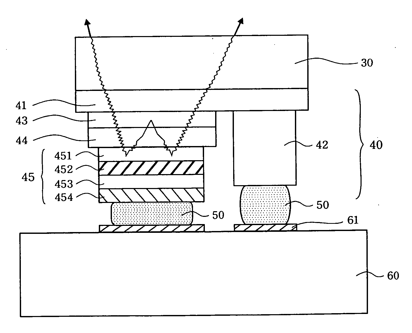
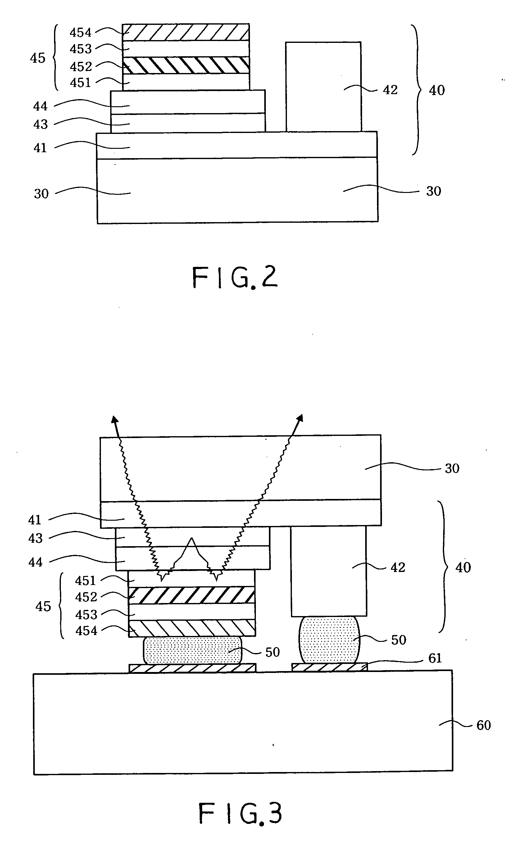
[0037] First of all, referring to FIG. 2, an embodiment of a light-emitting diode (LED) die includes a translucent substrate 30 and a semiconductor die structure 40.

[0038] In accordance with the invention, the translucent substrate 30 is preferably a sapphire substrate.

[0039] The semiconductor die structure 40 is attached on the translucent substrate 30 and made of group III nitride compound. The semiconductor die structure 40 includes a first type semiconductor layer 41 (e.g. n-type gallium nitride) formed on a top side of the translucent substrate 30. A first electrode 42 is formed on a top side of the first type semiconductor layer 41 acting as n-type gallium nitride. The first electrode 42 functions as n-electrode. An active layer 43 beside the first electrode 42 is formed on a top side of the first type semiconductor layer 41 without covering the first electrode 42. A second type semiconductor layer 44 acts as p-type gallium nitride and is formed on a top side of the active l...


PUM


Abstract

A flip-chip electrode light-emitting element formed by multilayer coatings where a translucent conducting layer and a highly reflective metal layer acts as flip-chip electrode for enhancing the LED luminous efficiency. The flip-chip electrode light-emitting element includes a translucent substrate, a semiconductor die structure attached on the translucent substrate and made of group III nitride compounds, and an intermediate layer adapted to support the inverted semiconductor die structure on a submount. The flip-chip electrode formed by multiplayer coatings includes a current-spreading transparent conducting layer formed on a top side of the second type semiconductor layer, a highly reflective metal layer formed on a top side of the transparent conducting layer, a metallic diffusion barrier layer formed on a top side of the highly reflective metal layer, and a bonding layer electrically coupled to the intermediate layer and formed on a top side of the barrier layer. Moreover, an ohmic contact layer is formed on the transparent conducting layer. And a passivation layer encloses the die structure for insulating p/n interface and for avoiding the creation of the leakage current.

Description

BACKGROUND OF THE INVENTION [0001] 1. Field of the Invention [0002] The invention relates to a flip-chip light-emitting diode (LED), and more particularly to a flip-chip electrode light-emitting element formed by multiplayer coatings for enhancing the current spreading function and for reflecting the light beam in the direction of the electrode to a translucent substrate. In this way, the luminous efficiency can be increased. [0003] 2. Description of the Related Art [0004] The lattice match is a significant task for the semiconductor LED. For the most of the III-V compound semiconductor, a good substrate for supporting an epitaxy layer is still unavailable. The lattice of the grew epitaxy layer has to match to that of the substrate for preventing photons from being absorbed by defective portions of the lattice damaged by the stress in the process. Otherwise, the luminous efficiency of the light-emitting diode would be considerably lowered. [0005] In addition, blue / green LEDs were ma...

Claims


Application Information

Patent Timeline
IPC IPC(8): H01L33/00H01L33/32H01L33/42H01L33/44H01L33/62
CPCH01L33/32H01L33/405H01L33/62H01L2224/16H01L2924/01046H01L2924/01078H01L2924/01079H01L2924/3025H01L2924/01019H01L2924/12041H01L2224/0508H01L2224/05573H01L2224/05568H01L2224/05023H01L2224/05001H01L2224/05124H01L2224/05139H01L2224/05155H01L2224/05164H01L2224/05166H01L2224/05169H01L2224/05184H01L2224/05611H01L2224/05644H01L2224/06131H01L2924/00014
Inventor LU, CHI-WEIHUANG, WEN-CHIEHCHANG, PAN-TZUWANG, JAMES
Owner ARIMA OPTOELECTRONICS
Why Eureka
Try Eureka