Thermoelectric cooling and/or moderation of transient thermal load using phase change material

a phase change material and thermal load technology, applied in the direction of domestic cooling devices, lighting and heating devices, semiconductor lasers, etc., can solve the problems of sensitivity being typically limited by background noise, most sensors, ccd's (and cmos devices) susceptible to noise, etc., and achieve the effect of avoiding large localized excursions

Inactive Publication Date: 2006-04-27
NANOCOOLERS
View PDF8 Cites 46 Cited by
  • Summary
  • Abstract
  • Description
  • Claims
  • Application Information

AI Technical Summary

Benefits of technology

[0012] In some configurations, a thermoelectric is employed in conjunction with the phase change material. For example, the thermoelectric may at least partially define a heat transfer path from the photoemissive device to the phase change material. Similar configurations may be employed for photosensitive devices. In such configurations, the phase change material may effectively clamp one side (typically the hot side) of the thermoelectric as heat transferred across the thermoelectric is absorbed into the transition of at least some of the phase change material from a first state thereof to a second state. The thermoelectric may be transiently operated in substantial synchrony with operation of the photoemissive or photosensitive device to provide extremely high density spot cooling when and where desired.
[0013] Alternatively (or additionally), phase change material may be disposed in close thermal proximity to the photoemissive device, absorbing substantial transient heat flux into the transition of at least some of the phase change material from a first state thereof to a second state. In this way, a phase change material (and an appropriate amount thereof) can be selected to absorb the transient heat flux generated or evolved by the photoemissive device, thereby avoiding large localized excursions in temperature of the device that may otherwise occur when the heat flux generated or evolved overwhelms conventional heat transfer pathways away from the photoemissive device. In some such configurations, the phase change material may be employed with a thermoelectric (e.g., between the photoemissive device and the thermoelectric). In some configurations, phase change material may be employed without a thermoelectric simply to moderate thermal transients generated by photoemissive device.

Problems solved by technology

Of course, like most sensors, CCD's (and CMOS devices) are susceptible to noise because the materials and device structures exhibit a baseline level of electron “action” (or current).
Sensitivity is typically limited by background noise.
Accordingly, as higher and higher pixel densities are supported (often with smaller and smaller sensor elements), sensitivity and noise issues may become increasingly important.
Most approaches to cooling flash LEDs and CCD have been limited to passive heat spreading packages.
Unfortunately, it is difficult to increase the performance of white LEDs and CCDs with known passive methods.

Method used


Image

  • Thermoelectric cooling and/or moderation of transient thermal load using phase change material
  • Thermoelectric cooling and/or moderation of transient thermal load using phase change material
  • Thermoelectric cooling and/or moderation of transient thermal load using phase change material

Examples


Embodiment Construction

)

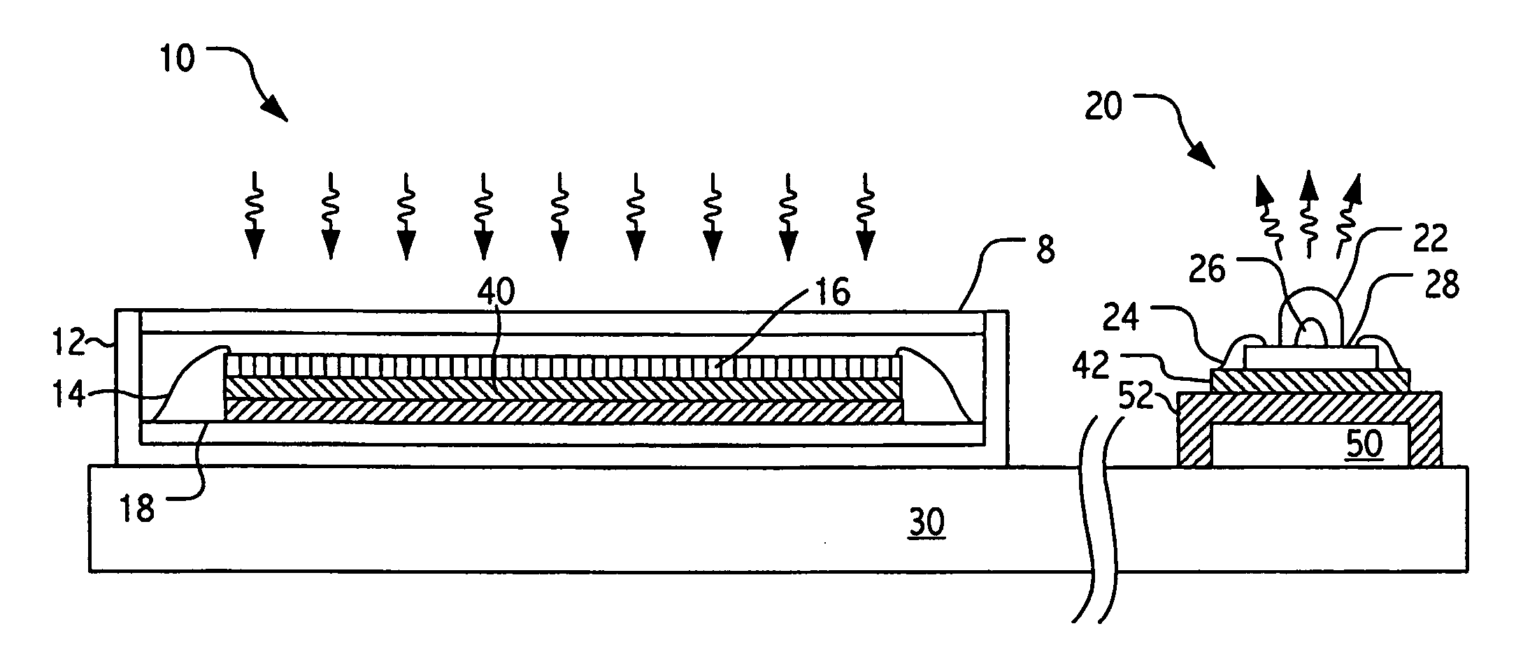
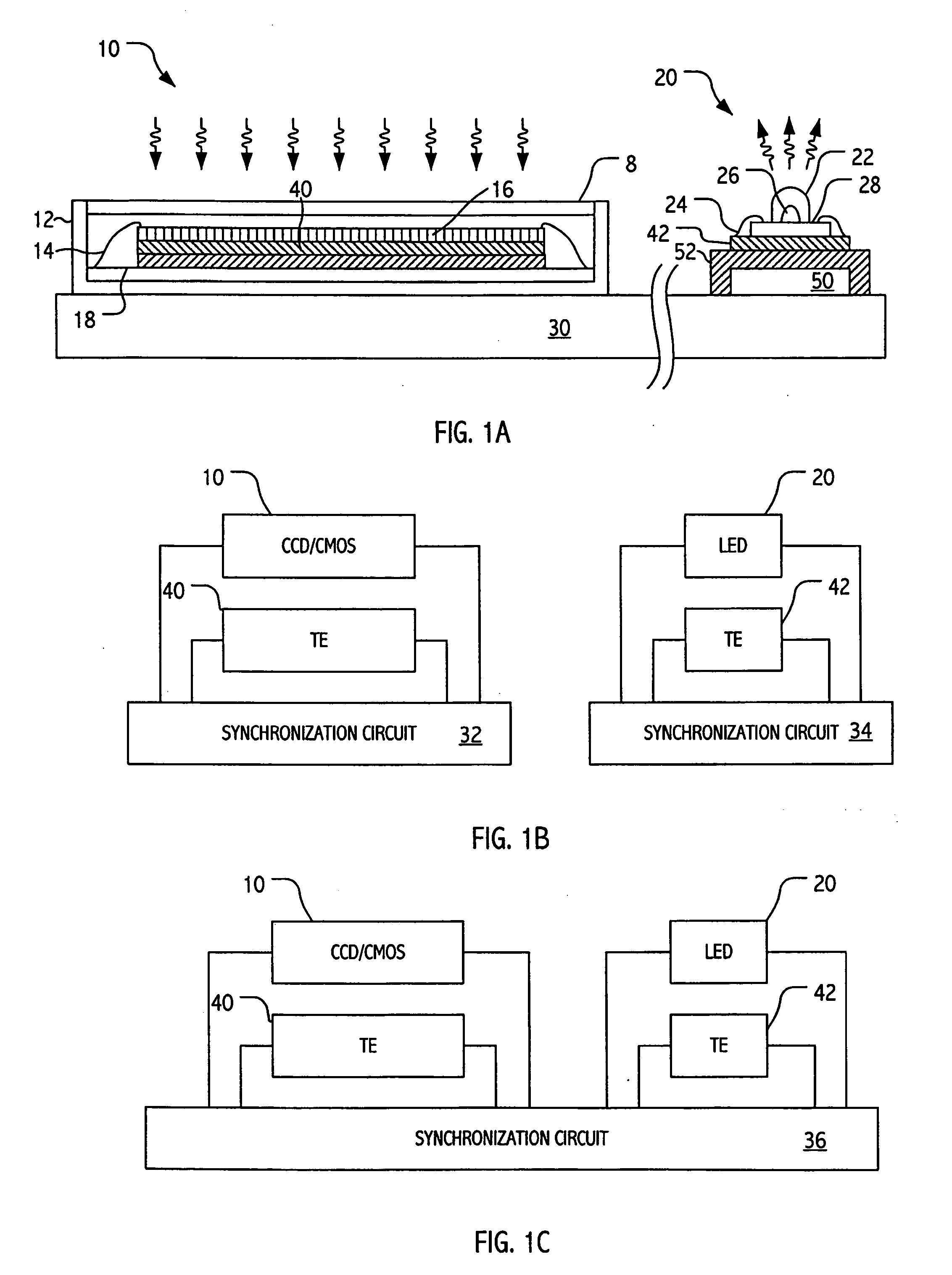
[0028] While not limited thereto, the invented techniques described and illustrated herein can permit high luminous flux and greater lifetimes for flash LEDs, and greater photon sensitivity and lower dark currents for CCD / CMOS imagers. Accordingly, we describe aspects of the inventive concepts in the context of configurations, optoelectronic devices, materials and heat fluxes typical of consumer electronics such as digital cameras and mobile phones that incorporate similar technologies. However, as more completely described herein, the invention is not limited to such exploitations.

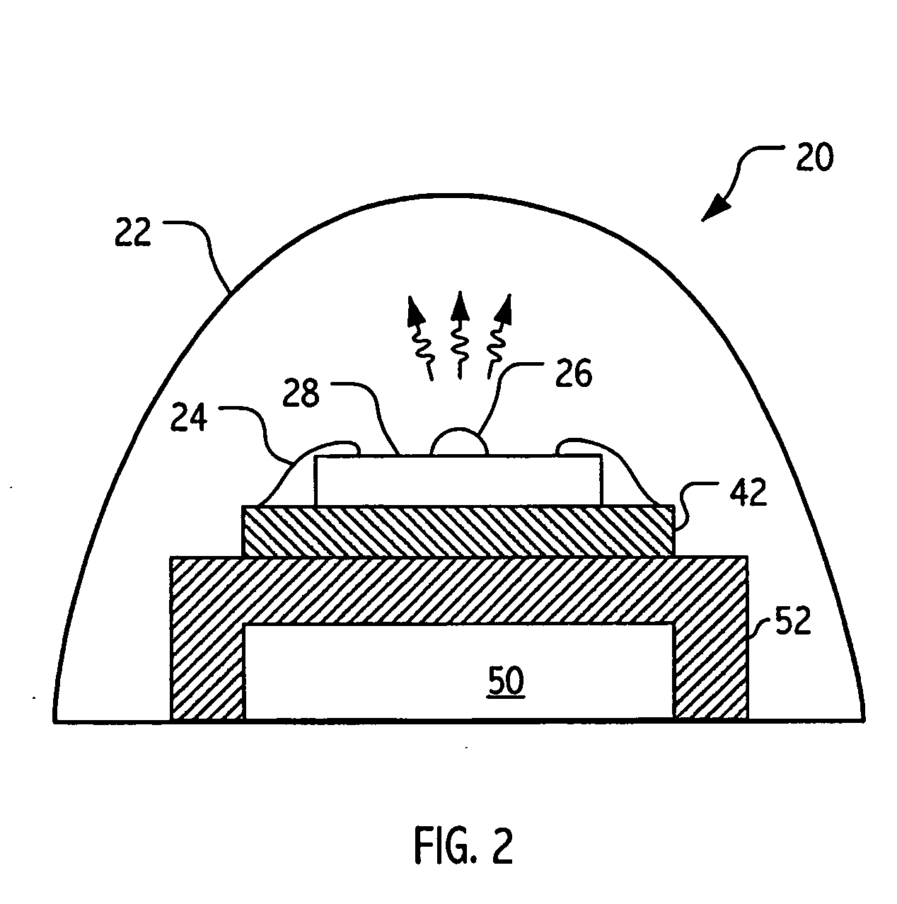
[0029] In particular, the description that follows emphasizes exploitations of the present invention in which a light emitting diode, e.g., a white LED, or other photoemissive device is used in a flash mode of operation, e.g., as flash illumination to support digital imaging. In such exploitations, extremely high transient thermal flux can be generated. Particularly for white LEDs, quality of the lumina...


PUM


Abstract

Techniques described and illustrated herein can permit high luminous flux and / or longer lifetimes for a class of photoemissive device configurations and / or uses that generate intense highly localized, but transient heat flux. For example, certain Light Emitting Diode (LED) applications, e.g., for flash illumination, certain solid state laser configurations and other similar configurations and uses may benefit from the developed techniques. In particular, it has been discovered that by locating an amount of appropriate phase change material in close thermal proximity to such a photoemissive device, substantial generated heat fluxes may be “absorbed” into a phase transition of the phase change material. In some configurations, a thermoelectric is employed in conjunction with the phase change material. For example, the thermoelectric may at least partially define a heat transfer path from the photoemissive device to the phase change material. Similar configurations may be employed for photosensitive devices. In such configurations, the phase change material may effectively clamp one side (typically the hot side) of the thermoelectric as heat transferred across the thermoelectric is absorbed into the transition of at least some of the phase change material from a first state thereof to a second state. The thermoelectric may be transiently operated in substantial synchrony with operation of the photoemissive or photosensitive device to provide extremely high density spot cooling when and where desired.

Description

CROSS-REFERENCE TO RELATED APPLICATION(S) [0001] This application claims benefit of U.S. Provisional Application No. 60 / 621,382 entitled “TRANSIENT THERMOELECTRIC COOLING OF OPTOELECTRONIC DEVICES,” filed on Oct. 22, 2004. [0002] In addition, this application is related to commonly-owned U.S. patent application Ser. No. ______ entitled “TRANSIENT THERMOELECTRIC COOLING OF OPTOELECTRONIC DEVICES,” and naming Uttam Ghoshal as inventor, filed on even date herewith, the entirety of which is incorporated herein by reference.BACKGROUND [0003] 1. Field of the Invention [0004] The present invention relates to management of transient thermal loads, such as exhibited by some optoelectronic devices, and particularly to thermoelectric cooling and / or moderation of transient thermal loads using phase change material. [0005] 2. Related Art [0006] Modern digital devices including consumer electronics increasingly employ optoelectronic devices. Digital cameras (as well as phones that include camera ...

Claims


Application Information

Patent Timeline
Patent Type & Authority Applications(United States)
IPC IPC(8): F25B21/02F25D23/12
CPCF25B21/02F25B2321/021F25B2321/025H01L31/024H01L33/645H01S5/02228H01L2224/48091H01S5/02469H05K1/0204H05K2201/10106H01L2924/00014H01S5/02234
Inventor GHOSHAL, UTTAM
Owner NANOCOOLERS
Why Eureka
Try Eureka