Method for producing multilayer printed wiring board, multilayer printed wiring board, and electronic device

a multi-layer printed wiring board and printed technology, applied in the direction of superimposed coating process, resistive material coating, liquid/solution decomposition chemical coating, etc., can solve the problem of difficult to achieve fine conductor pattern, difficult to position, entail the same problems, etc., to achieve high reliability and high reliability through-hole conductor

Inactive Publication Date: 2006-04-27
SHARP KK
View PDF7 Cites 2 Cited by
  • Summary
  • Abstract
  • Description
  • Claims
  • Application Information

AI Technical Summary

Benefits of technology

[0045] This configuration makes it possible to achieve a highly reliable electronic device

Problems solved by technology

In addition, as the land portion becomes smaller, positioning becomes more difficult.
This method also entails the same problems as Patent documents 1 and 2.
When forming a conductor pattern using a conventional etching method, it is difficult to achieve a fine conductor pattern beyond a certain point due to an issue of aspect ratio between the line width and film thickness of a conductor pattern.
In addition, when forming a conductor pattern through etching, it is difficult to change the etching speed ratio between the depth direction and plane direction of the conductor pattern.
For this reason, it has not been easy to form a conductor pattern with a line width smaller than the film thickness of the conductor pattern.
However, the film thickness of a through-hole conductor can become smaller than the film thickness of a panel plating layer depending on conditions such as the state of the wall surface of the through-hole and the flow of plating fluid, and often varies due to unstable deposition of a plating metal.
Accordingly, the film thickness of a panel plating layer cannot be reduced too much, in view of the heat stress to be applied during the use of the multilayer printed wiring board and at the time of mounting electronic components, reliability in a

Method used


Image

  • Method for producing multilayer printed wiring board, multilayer printed wiring board, and electronic device
  • Method for producing multilayer printed wiring board, multilayer printed wiring board, and electronic device
  • Method for producing multilayer printed wiring board, multilayer printed wiring board, and electronic device

Examples


embodiment 1

[0061] FIGS. 1 to 5 are cross-sectional views in process for explaining a multilayer printed wiring board and a method for producing the same according to Embodiment 1 of the present invention.

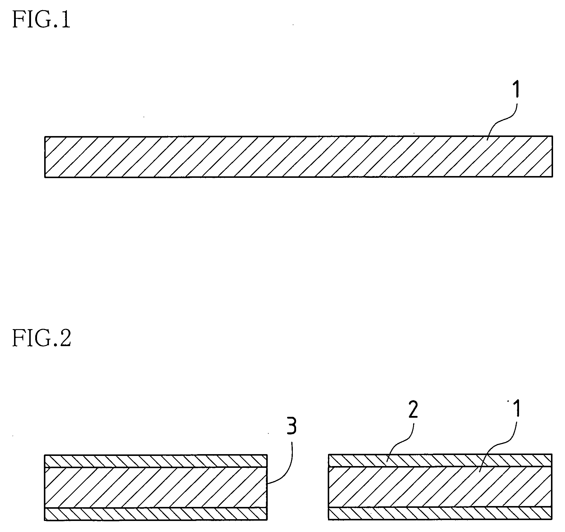
[0062]FIG. 1 shows a wiring board substrate 1, which is a core material of a multilayer printed wiring board according to the present invention. The wiring board substrate 1 is constituted by an insulating resin plate that is generally available in the market. Although a material such as epoxy resin, polyester resin, fluororesin and polyimide resin is generally used for the resin plate, it is needless to say that other materials may be used. In addition, to secure the physical strength, a fiber-reinforced resin plate, which is reinforced with fibers such as paper, fiber glass and aramid fiber, is preferable as the resin plate.

[0063] Furthermore, in view of simplification of production process, a resin plate processed with a plating catalyst, which has a plating catalyst mixed into the resin ...

embodiment 2

[0083]FIG. 6 is a cross-sectional view for explaining an electronic device according to Embodiment 2 of the present invention. The same numeric references are used for the same components as Embodiment 1 and detailed explanation is omitted when deemed appropriate.

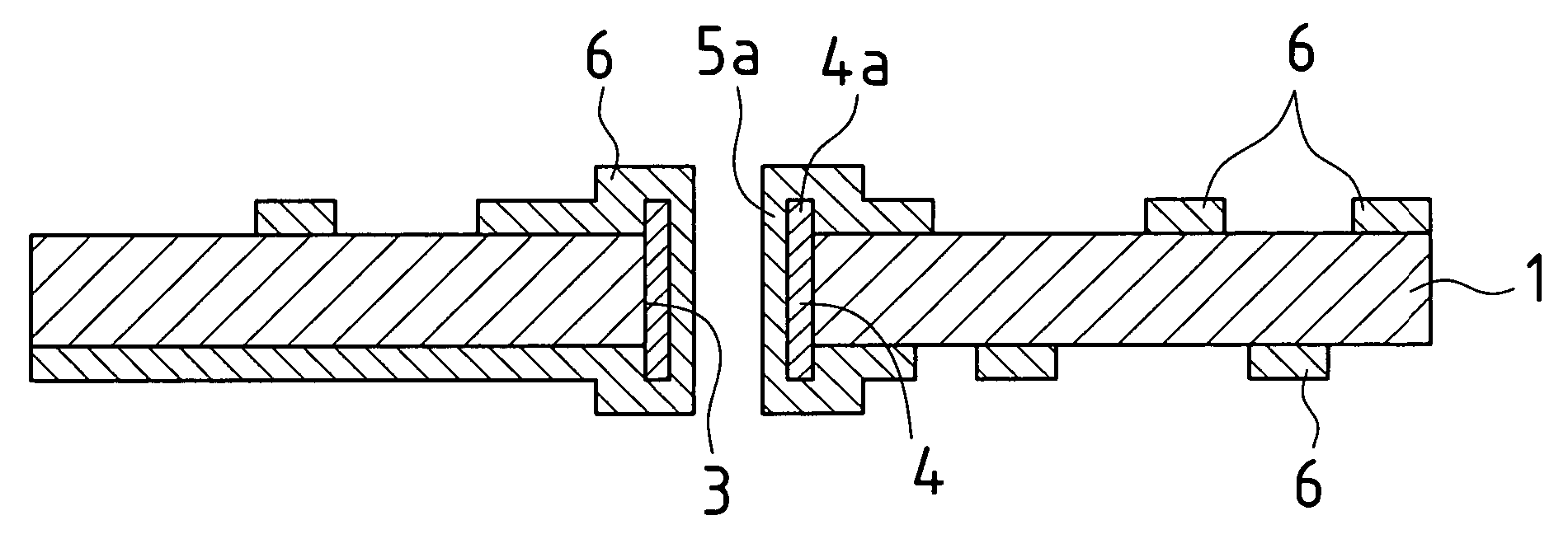
[0084]FIG. 6 indicates a conceptual illustration of an electronic device having electronic components 7 mounted (soldered) as appropriate thereon on locations that correspond to the conductor pattern 6 (multilayer printed wiring board formed according to Embodiment 1 as shown in FIG. 5) which is formed to correspond to specific circuit wiring for construction of the electronic device. Examples of the electronic components 7 include chip resistors and chip capacitors. It is, of course, also possible to mount a chip integrated circuit.

[0085] Since an electronic device is produced by mounting the electronic components 7 on a more reliable multilayer printed wiring board having the through-hole conductor 4 (and the panel-plat...

embodiment 3

[0086]FIG. 7 is a cross-sectional view for explaining a multilayer printed wiring board and a method for producing the same according to Embodiment 3 of the present invention. The same numeric references are used for the same components as Embodiments 1 and 2 and detailed explanation is omitted when deemed appropriate.

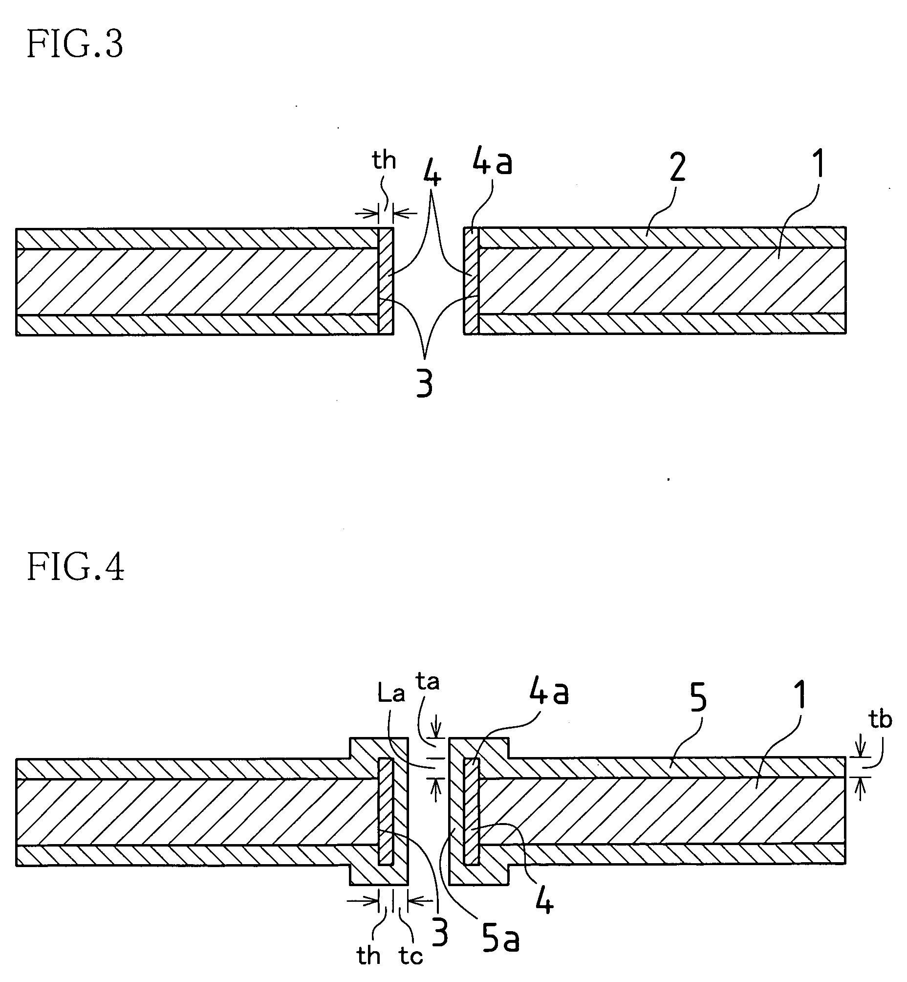
[0087] A multilayer printed wiring board in this embodiment is produced by changing the plating conditions used to form the panel plating layer 5 (see FIG. 4) in a panel plating layer forming process according to Embodiment 1 so that the film thickness tb of the panel plating layer 5 becomes in the same level as the sum of the protrusion length La of the protrusion 4a of the through-hole conductor 4 and the film thickness ta of the panel plating layer 5. The plating conditions include composition of a panel plating bath, plating method, metal selection and plating film thickness.

[0088] Film thickness tb of the panel plating layer 5 may be set to the film thickness ne...


PUM

PropertyMeasurementUnit
Thicknessaaaaaaaaaa
Electrical conductoraaaaaaaaaa
Areaaaaaaaaaaa

Abstract

A plating resist film 2 is formed on a wiring board substrate 1 as a core material of a multilayer printed wiring board, then a through-hole 3 is formed, and through-hole conductor 4 is formed along the wall surface of the through-hole 3 and the through-hole surface of the plating resist film 2, so that protrusion portion 4a is formed in the through-hole conductor 4. The plating resist film 2 is then stripped off and a panel plating layer 5 is formed on the surface of the wiring board substrate 1 and the through-hole conductor 4 so that the through-hole 4 and the panel plating layer 5 are connected with the protrusion 4a coated, and thus the connection area can be increased.

Description

BACKGROUND OF THE INVENTION [0001] This application claims priority under 35 U.S.C. § 119 (a) on Patent Application No. 2004-312520 filed in Japan on Oct. 27, 2004, the entire contents of which are hereby incorporated by reference. [0002] The present invention relates to a method for producing a multilayer printed wiring board that improves the reliability of through-hole conductor formed on a multilayer printed wiring board, a multilayer printed wiring board, and an electronic device using such a multilayer printed wiring board. [0003]FIGS. 13 and 14 are cross-sectional views in a process for explaining a multilayer printed wiring board of Conventional example 1 and a method for producing the same. [0004]FIG. 13 shows a base material of a multilayer printed wiring board of Conventional example 1. For the base material of the multilayer printed wiring board, a commercially available laminate having copper coating on both its sides, more specifically a laminate having a copper foil a...

Claims


Application Information

Patent Timeline
IPC IPC(8): H05K1/11H05K3/42
CPCH05K1/116H05K3/184H05K3/426Y10T29/49165H05K2201/0166H05K2201/09736Y10T29/49126H05K3/427
Inventor UENO, YUKIHIRO
Owner SHARP KK
Why Eureka
Try Eureka