Method for making a passivated semiconductor substrate
- Summary
- Abstract
- Description
- Claims
- Application Information
AI Technical Summary
Benefits of technology
Problems solved by technology
Method used
Image

Examples
example 1
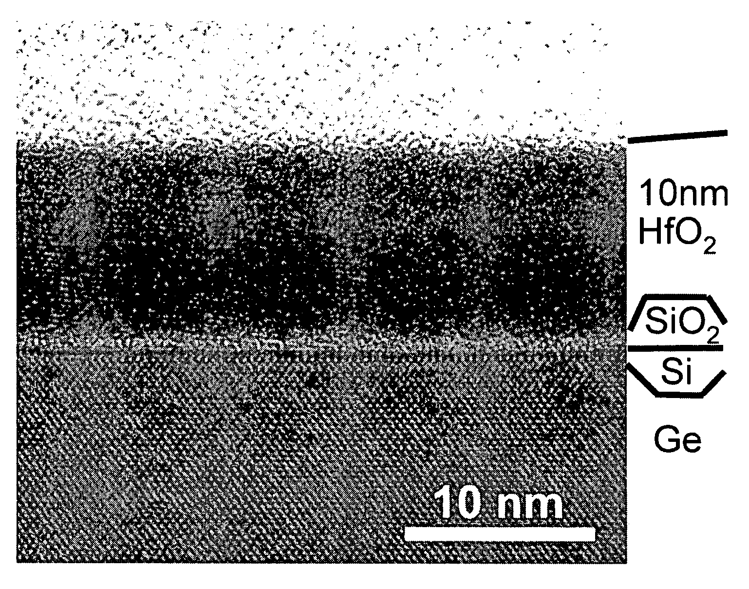
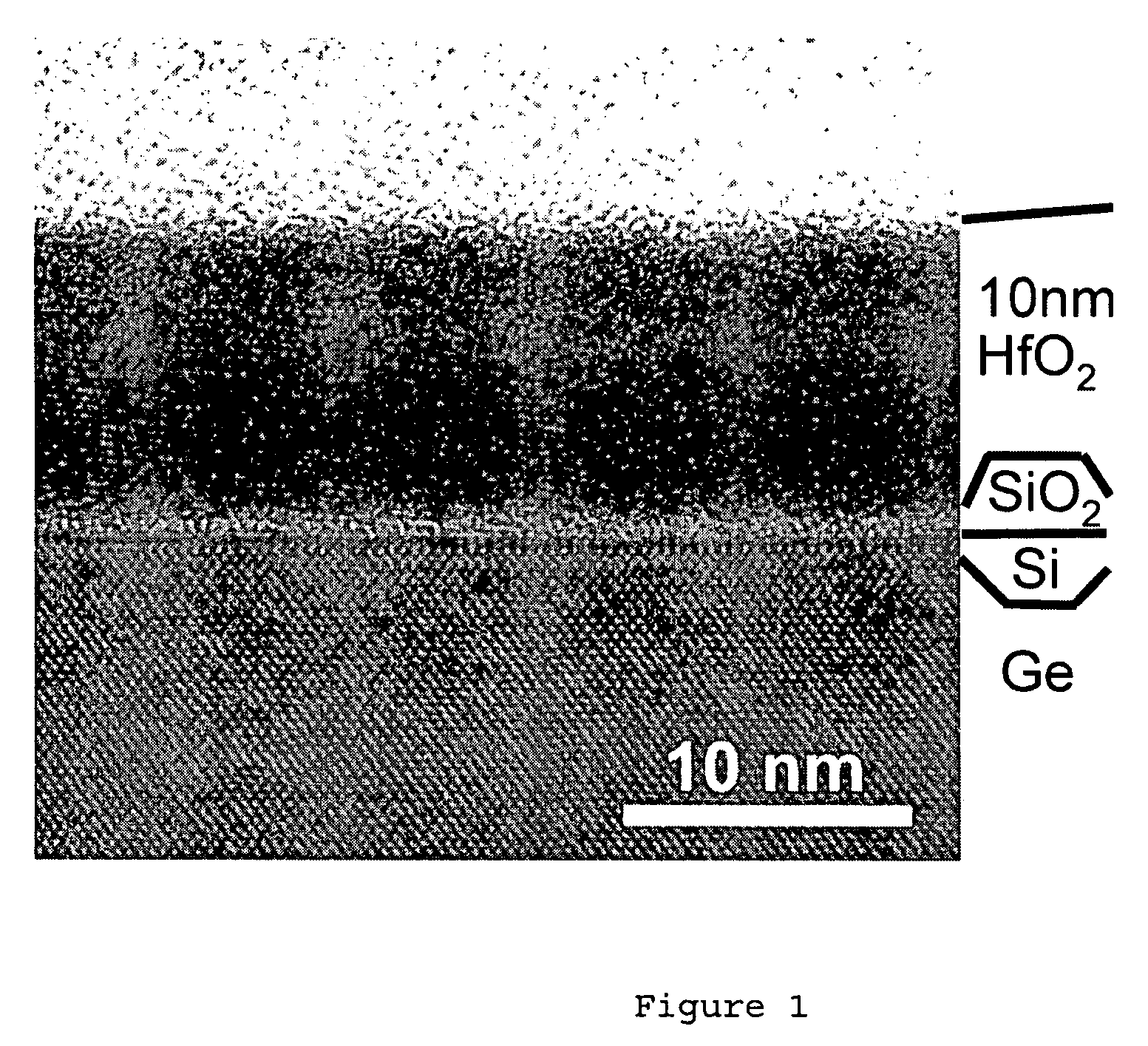
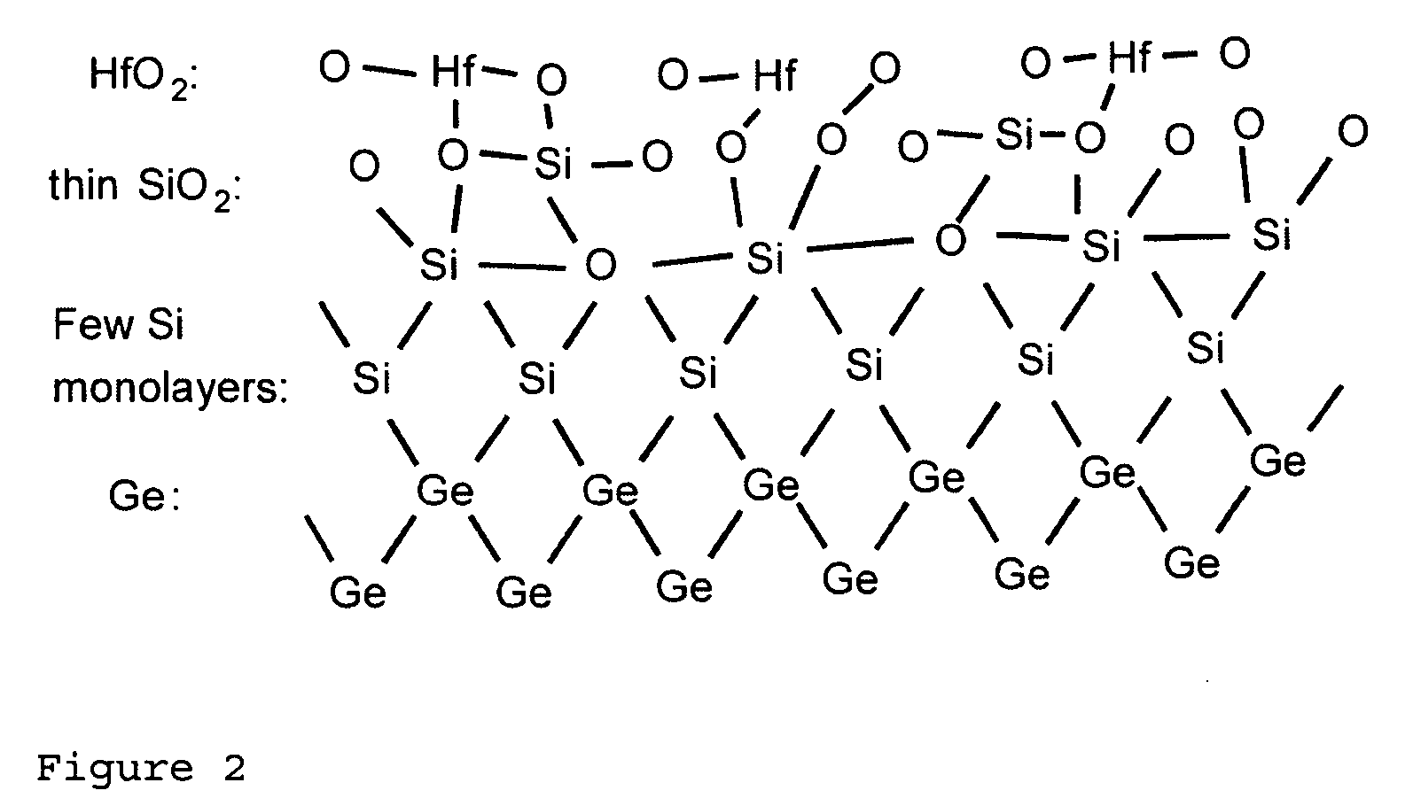
[0044] In order to make a Ge capacitor, a gate stack is deposited on top of the Ge channel. To avoid a high interface state density at the interface between the Ge channel and the gate oxide, the Ge surface is passivated by forming a substantially lattice matched monolayer of silicon on top of it. This is done by growing a few monolayers of mono-crystalline silicon in an epireactor, e.g. ASM epsilon, at a temperature between 500 and 575° C., with 20 to 50 sccm silane, a pressure of 40 torr (53.3 mbar) and 10 to 40 slm N2 as carrier gas. This mono-crystalline silicon layer is formed substantially lattice matched to the Ge.
[0045] In order to be able to grow epitaxially on the Ge surface and to remove substantially all germanium oxide on top of it, a surface preparation is done. Therefore, the Ge surface is subjected to a 1% HF solution, followed by anneal in H2 ambient inside the chamber of the epireactor at a temperature between 650 and 850° C.
[0046] After the mono-crystalline grow...
example 2
[0051] In the case of Spreading Resistance analysis, e.g., SRP (Spreading Resistance Probing) and SSRM (Scanning Spreading Resistance Microscopy), on doped Ge substrates, point contacts are realized between the metal probe and the Ge surface. When contacting the Ge directly with the probe, a Shottky contact is created due to generation of a depletion layer at the Ge side. When passivating the doped Ge substrate with a mono-crystalline undoped silicon layer of the preferred embodiments, the Shottky contact is modified into a substantially Ohmic contact. FIG. 8 proofs that doped Ge samples with an epitaxially grown mono-crystalline silicon layer of two monolayers thickness show an approximately Ohmic current-voltage profile compared to the samples without silicon layer. This simplifies Spreading Resistance analysis and improves its accuracy to a high extend.
PUM
 Abstract
Description
Claims
Application Information
 - R&D Engineer
- R&D Manager
- IP Professional
- Industry Leading Data Capabilities
- Powerful AI technology
- Patent DNA Extraction
Browse by: Latest US Patents, China's latest patents, Technical Efficacy Thesaurus, Application Domain, Technology Topic.
© 2024 PatSnap. All rights reserved.Legal|Privacy policy|Modern Slavery Act Transparency Statement|Sitemap