Eureka AIR delivers breakthrough ideas for toughest innovation challenges, trusted by R&D personnel around the world.

Method for producing piezoelectric actuator and method for producing ink-jet head

Inactive Publication Date: 2006-05-04
BROTHER KOGYO KK
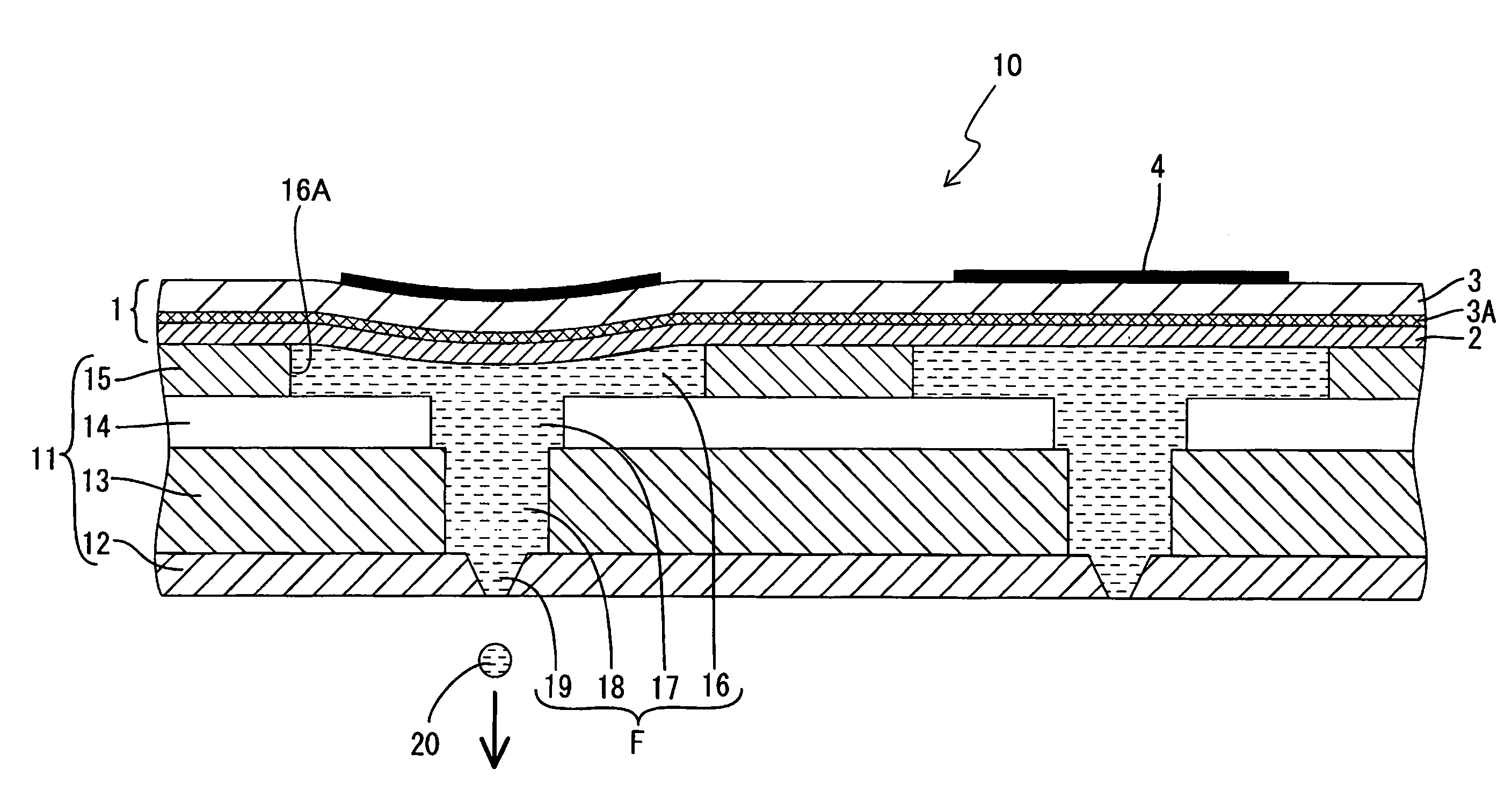
View PDF4 Cites 10 Cited by
  • Summary
  • Abstract
  • Description
  • Claims
  • Application Information

AI Technical Summary

Benefits of technology

[0007] The present invention has been made in view of the above-mentioned situations. An object of the present invention is to provide a method for manufacturing a piezoelectric actuator and an ink-jet head capable of improving the piezoelectric characteristic.
[0017] The diffusion layer formation process is described below. When a piezoelectric film is exposed to high-temperature environment by annealing, the easily diffusing elements contained in the substrate diffuse gradually into the piezoelectric film and a diffusion layer is formed on the interface between the piezoelectric film and the substrate. As the annealing time becomes longer, this diffusion layer grows gradually in the thickness direction of the piezoelectric film. However, when the inventor further studied the relationship between the diffusion layer and piezoelectric characteristic, the inventor has found that the degradation of piezoelectric characteristic caused by this diffusion depends on the ratio of the thickness of the diffusion layer to the thickness of the entire piezoelectric film and when the ratio (L1 / L2) of the thickness L2 of the diffusion layer to the thickness L1 of the entire piezoelectric film is about 0.02 or less, a piezoelectric characteristic of 80-90% or more of that without the diffusion can be ensured.
[0018] Accordingly, the inventor has conducted a comprehensive study of annealing conditions for obtaining a sufficient piezoelectric characteristic, while minimizing the thickness of the diffusion layer. Here, the growth of piezoelectric body grain and correction of lattice defects (slip, stacking faults, dislocations) resulting from impact shock occurring when the blown particles collide on the substrate during film formation are necessary to improve the piezoelectric characteristic. In this case, the annealing treatment has to be conducted under certain high-temperature conditions to provide for grain growth. On the other hand, the annealing treatment has to be conducted at a constant temperature and the annealing treatment has also to be conducted during a certain recovery period to correct the lattice defects. Accordingly, the inventor found that in the initial stage of annealing, the treatment is conducted for a short time at a high temperature to ensure grain growth, and then the lattice defects presenting the crystal can be corrected by conducting annealing for a certain time at a certain low temperature at which diffusion can be inhibited. The present invention is based on this finding.
[0021] In addition, in the first annealing step, the temperature of the treatment atmosphere may be raised to the predetermined annealing temperature as fast as possible after the annealing is started in order to cause the necessary grain growth as short a time as possible. More specifically, the temperature may be raised at a temperature rise rate of not less than 800° C. / min. Furthermore, in the first annealing step, the substrate can be placed into the treatment atmosphere after the temperature of the treatment atmosphere previously has been raised to the annealing temperature.
[0031] In the method for manufacturing the piezoelectric actuator and the ink-jet head in accordance with the present invention, the annealing treatment of the piezoelectric actuator is conducted in two steps: the first annealing step and the second annealing step conducted at a temperature lower and for a time longer than those of the first annealing step. With such treatment, grain growth inside the piezoelectric film can be sufficiently induced, while minimizing the diffusion layer growth, by the first annealing step conducted at a high temperature within a short interval, and then lattice defects in the piezoelectric film can be sufficiently corrected, while inhibiting the diffusion layer growth, by the second annealing in which the piezoelectric film is annealed at a low temperature and for a long time. Therefore, in the method for manufacturing the piezoelectric actuator and ink-jet head in accordance with the present invention, the piezoelectric characteristic can be sufficiently improved, while minimizing the growth of diffusion layer in the piezoelectric film.
[0032] Furthermore, when the temperature is raised as fast as possible to the annealing temperature in the first annealing step in accordance with the present invention, or when the temperature of the treatment atmosphere is previously raised to the annealing temperature and then the substrate is placed into the treatment atmosphere and annealing is conducted, the annealing treatment can be conducted at a high temperature enabling grain growth in the piezoelectric film for as long a time as possible within a range in which the diffusion layer is reduced to a minimum. Therefore, the piezoelectric characteristic can be sufficiently improved.

Problems solved by technology

Therefore, a piezoelectric film having a sufficient piezoelectric characteristic cannot be obtained by the size reduction of the particles and occurrence of lattice defects due to collisions.
However, when the inventor actually formed a piezoelectric layer on a substrate by the AD method and then conducted annealing, the piezoelectric characteristic degraded.

Method used


Image

  • Method for producing piezoelectric actuator and method for producing ink-jet head
  • Method for producing piezoelectric actuator and method for producing ink-jet head
  • Method for producing piezoelectric actuator and method for producing ink-jet head

Examples


example 1

[0105] In Example 1, a piezoelectric film (PZT) with a thickness of 7 μm was formed on a substrate (SUS430) in the same manner as in the above-described preparatory tests. Then, the substrate with the piezoelectric film formed thereon was introduced into a muffler furnace with a temperature raised to 850° C. and held for 1 min (this process is the first annealing step).

[0106] Then, the substrate was transferred to another muffler furnace with a temperature raised to 700° C. and held therein for 3 min. The substrate was thereafter transferred to another muffler furnace with a temperature raised to 600° C., held therein for 5 min, then transferred to another muffler furnace with a temperature raised to 500° C., and held therein for 15 min (this process is the second annealing step). The substrate was then removed from the furnace and cooled to room temperature by natural cooling. A piezoelectric actuator was then constructed in the same manner as in the preparatory tests.

[0107] The ...

example 2

[0109] In Example 2, a piezoelectric film (PZT) with a thickness of 9 μm was formed on a substrate (SUS430) in the same manner as in the preparatory tests.

[0110] Then, the piezoelectric film surface was irradiated for 2 min by using an infrared lamp (manufactured by Inkridge Co., HSH-1). In this process, the irradiation intensity was adjusted so that the surface temperature of the piezoelectric film becomes about 1000° C. (this process is the first annealing step).

[0111] Then, the piezoelectric film was irradiated was for 5 min after the irradiation intensity was adjusted so that the piezoelectric film surface has a temperature of about 600° C. Then, the piezoelectric film was irradiated for 10 min after the irradiation intensity was adjusted so that the piezoelectric film surface has a temperature of about 500° C. (this process is the second annealing step). The piezoelectric film was then cooled to room temperature by natural cooling. The piezoelectric actuator was then construc...

example 3

[0114] In example 3, PZT added with Nb was used as a material for forming the piezoelectric film. In Example 3, first, a piezoelectric film with a thickness of 7 μm was formed on a substrate (SUS430) in the same manner as in the preparatory tests. Then, this piezoelectric film was subjected to annealing under the same conditions as in Example 1. Then, a piezoelectric actuator was constructed in the same manner as in Example 1.

[0115] The piezoelectric actuator fabricated in this example was tested in the same manner as in the preparatory tests. The applied electric field in the polarization treatment was 150 kV / cm.

[0116] As a result, the coercive electric field Ec was 35 kV / cm, the residual polarization Pr was 24 μC / cm2, and Pr / Ec was 0.69. A good piezoelectric characteristic was thus obtained.


PUM

PropertyMeasurementUnit
Temperatureaaaaaaaaaa

Abstract

In the annealing step of the method for manufacturing a piezoelectric actuator, the annealing in conducted in two steps: a first annealing step; and a second annealing step conducted at a temperature lower and for a time longer than those of the first annealing step. With such treatment, first, grain growth inside the piezoelectric film can be sufficiently induced, while minimizing the diffusion layer growth, by the first annealing step conducted at a high temperature within a short interval, and then lattice defects in the particles can be sufficiently corrected, while preventing the diffusion layer growth, by the second annealing step conducted at a temperature lower and for a time longer than those of the first annealing step. Accordingly, the piezoelectric characteristic can be improved by sufficiently conducting annealing, while restricting the thickness of the diffusion layer to a range where the piezoelectric characteristic is not affected.

Description

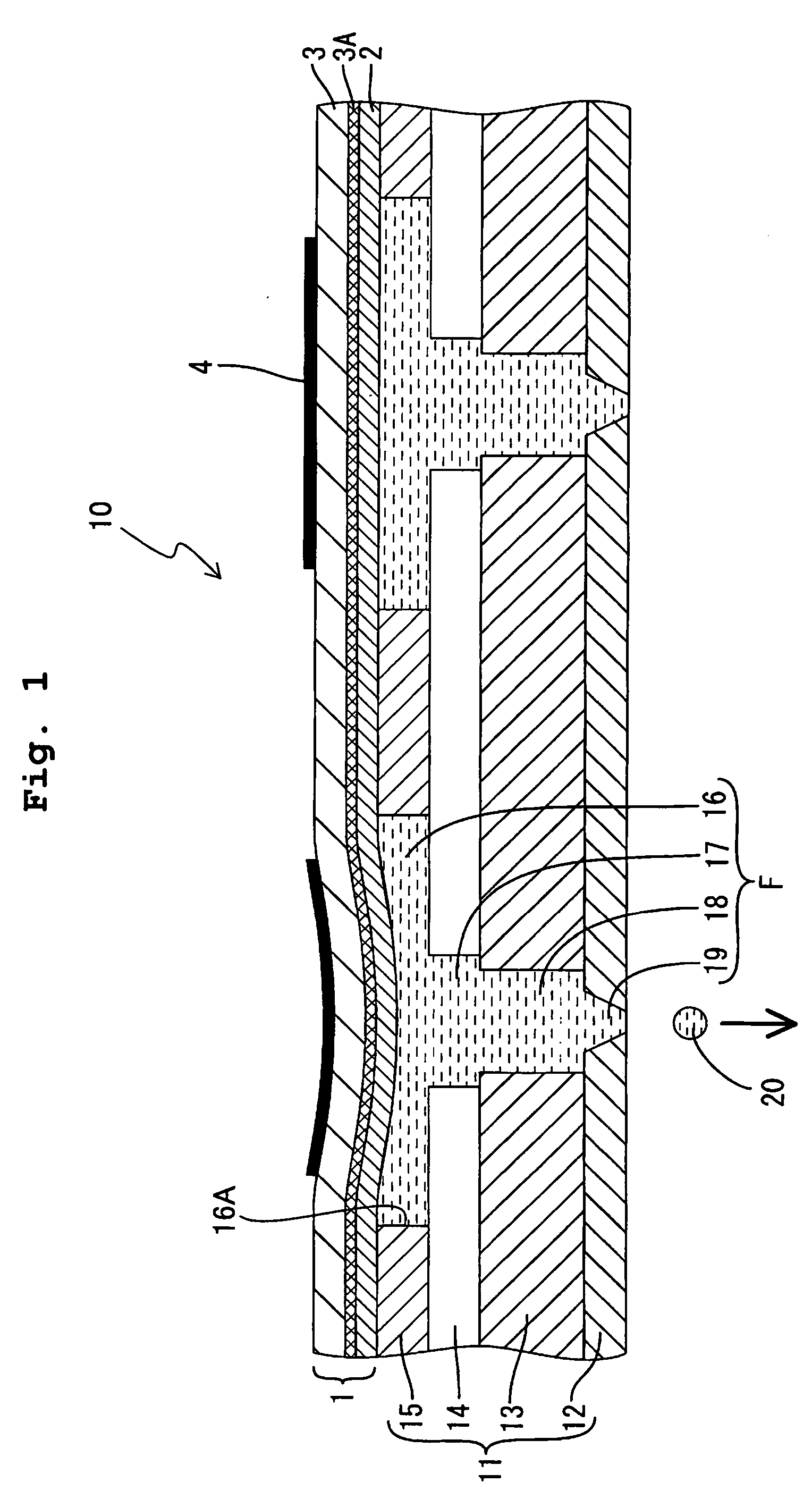
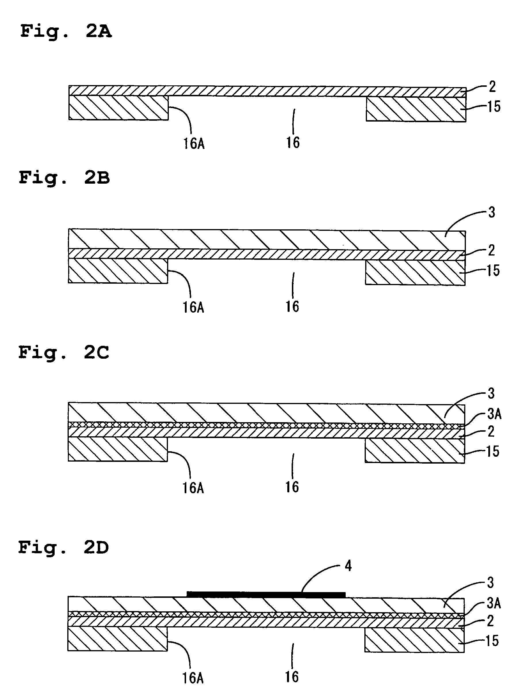
BACKGROUND OF THE INVENTION [0001] 1. Field of the Invention [0002] The present invention relates to a method for manufacturing a piezoelectric actuator and an ink-jet head. [0003] 2. Description of the Related Art [0004] An example of a piezoelectric actuator for an ink-jet head is disclosed in Japanese Patent Application Laid-open No. 11-314365. This piezoelectric actuator comprises a substrate (elastic film) provided so as to close the openings in pressure chambers communicated with nozzle openings in a channel forming body of the ink-jet head and has a structure in which a lower electrode, a piezoelectric film, and an upper electrode are laminated in this order on the substrate. When an electric field is applied between the lower electrode and upper electrode, the substrate bends by the deformation of the piezoelectric film, a pressure is applied to the ink present inside the pressure chambers, and the ink is discharged from the nozzle openings. [0005] A method called an aerosol...

Claims


Application Information

Patent Timeline
IPC IPC(8): B21D53/76H01L41/09B41J2/14B41J2/145B41J2/16H01L41/18H01L41/187H01L41/22H01L41/314H01L41/43
CPCB41J2/161B41J2/1623B41J2/1626B41J2/1631B41J2002/14266Y10T29/42H01L41/0973H01L41/1876H01L41/314Y10T29/49401H01L41/081H10N30/2047H10N30/8554H10N30/074H10N30/706
Inventor YASUI, MOTOHIRO
Owner BROTHER KOGYO KK
Why Eureka
Eureka Blog
Learn More