

Nitride based semiconductor device using nanorods and process for preparing the same
a technology of nanorods and semiconductors, which is applied in the manufacture of semiconductor/solid-state devices, semiconductor devices, electrical devices, etc., can solve the problems of significant deterioration of the performance of the device manufactured using, unsuitable mass production, and difficulty in large-diameter substrate production, so as to achieve the effect of reducing thermal stress
- Summary
- Abstract
- Description
- Claims
- Application Information
AI Technical Summary
Benefits of technology
Problems solved by technology
Method used
Image

Examples
Embodiment Construction
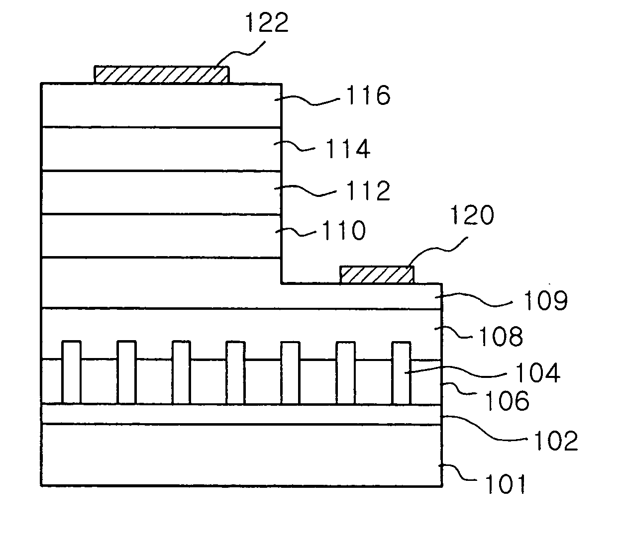
[0029] The present invention now will be, described more fully with reference to the accompanying drawings, in which embodiments of the invention are shown. The present invention may, however, be embodied in many different forms and should not be construed as being limited to the embodiments set forth herein; rather, these embodiments are provided so that this disclosure will be thorough and complete, and will fully convey the concept of the invention to those skilled in the art. Therefore, in the drawings, shape and size of some elements may be exaggerated for clarity, and like numbers refer to like elements throughout.
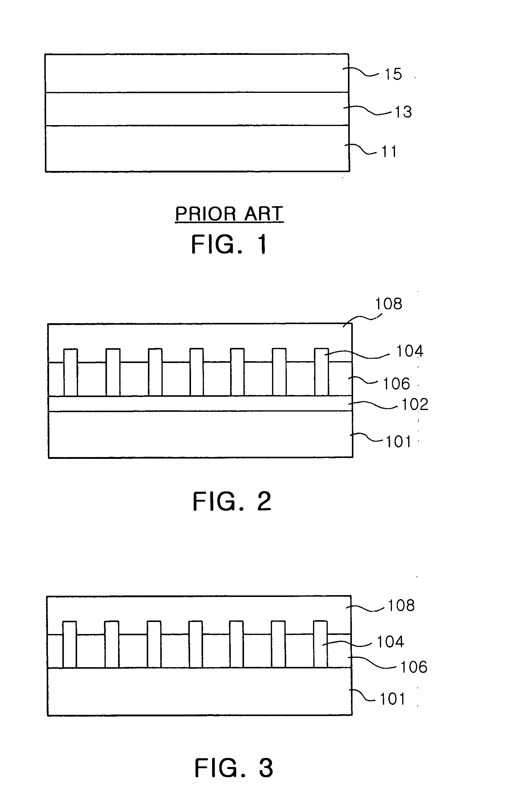
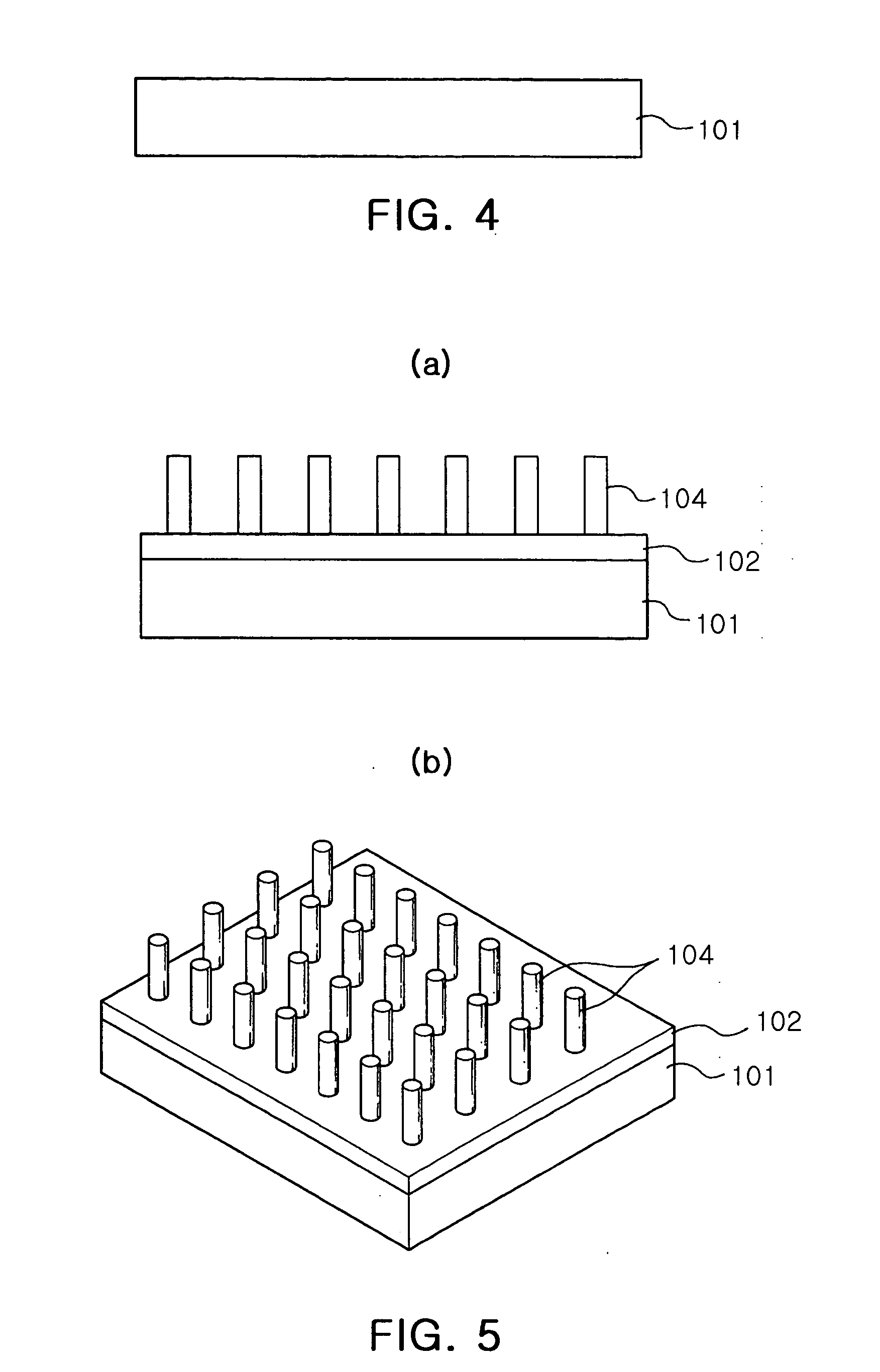
[0030]FIG. 2 is a view schematically showing a cross-sectional structure of a nitride based semiconductor device in accordance with one embodiment of the present invention. Referring to FIG. 2, a ZnO buffer layer 102, obtained by low-temperature growth, was formed on a Si. substrate 101. A plurality of nanorods 104 made of ZnO was aligned on the ZnO buffer layer 102...
PUM
 Abstract
Description
Claims
Application Information