Semiconductor substrate, semiconductor device, method of manufacturing semiconductor substare and method of manufacturing semiconductor device

a semiconductor device and semiconductor technology, applied in semiconductor devices, semiconductor/solid-state device details, electrical devices, etc., can solve the problems of short channel effect, high manufacturing cost, and long manufacturing time, so as to reduce the parasitic capacitance of the source/drain layer, prevent an increase in manufacturing cost, and suppress the effect of short channel

Inactive Publication Date: 2006-05-04
SEIKO EPSON CORP
View PDF20 Cites 10 Cited by
  • Summary
  • Abstract
  • Description
  • Claims
  • Application Information

AI Technical Summary

Benefits of technology

[0014] According to the above-mentioned structure, it is possible to make a BOX layer having SOI transistors formed thereon to have a non-uniform thickness, without using the SIMOX technique. Thus, it is possible to prevent an increase in manufacturing costs, and to achieve transistors capable of operating at high speed with low power consumption.
[0016] According to the above-mentioned structure, a BOX layer can be formed to have a small thickness below the channel and to have a large thickness below the source / drain layers, without using the SIMOX technique. Therefore, it is possible to suppress a short channel effect and to reduce parasitic capacitance of the source / drain layers. As a result, it is possible to achieve transistors capable of operating at high speed with low power consumption.
[0018] According to the above-mentioned method, it is possible to make the second semiconductor layer have a non-uniform thickness, corresponding to the first semiconductor layer having a non-uniform thickness. In addition, it is possible to make a BOX layer have a non-uniform thickness, without damaging the crystal quality of the second semiconductor layer. Accordingly, SOI transistors can be formed on an oxide film having a non-uniform thickness, without using the SIMOX technique. Thus, it is possible to prevent an increase in manufacturing costs, and to achieve transistors capable of operating at high speed with low power consumption.
[0020] According to the above-mentioned structure, it is possible to remove the first semiconductor layer with the second semiconductor layer remaining, and to reduce the thickness of the second semiconductor layer at the edge thereof. Accordingly, a BOX layer can be formed to have a small thickness below the cannel and to have a large thickness below the source / drain layers, without damaging the crystal quality of the second semiconductor layer. Thus, it is possible to suppress a short channel effect and to reduce parasitic capacitance of the source / drain layers, without using the SIMOS technique. As a result, it is possible to prevent an increase in manufacturing costs, and to achieve transistors capable of operating at high speed with low power consumption.
[0022] In this way, it is possible to increase the etching amount of the first semiconductor layer at the edge thereof, and to reduce the etching amount of the first semiconductor layer at the center thereof. As a result, it is possible to make the thickness of the first semiconductor layer uniform at the center thereof, and to reduce the thickness of the first semiconductor layer at the edge thereof.
[0024] According to the above-mentioned structure, it is possible to make the second semiconductor layer have a non-uniform thickness, corresponding to the first semiconductor layer having a non-uniform thickness. Accordingly, a BOX layer can be formed to have a small thickness below the cannel and to have a large thickness below the source / drain layers, without damaging the crystal quality of the second semiconductor layer. Thus, it is possible to suppress a short channel effect and to reduce parasitic capacitance of the source / drain layers, without using the SIMOS technique. As a result, it is possible to prevent an increase in manufacturing costs, and to achieve transistors capable of operating at high speed with low power consumption.

Problems solved by technology

Further, in the method disclosed in Japanese Unexamined Patent Application Publication No. 7-78994, a BOX layer having a non-uniform thickness is prepared by changing energy required for implanting oxygen ions.
However, the method disclosed in Japanese Unexamined Patent Application Publication Nos. 7-335898 has problems in that oxygen ions should be implanted into the semiconductor substrate with a dosage of 1E17 to 1E18 cm−2 and a longer manufacturing time and a high manufacturing cost are required.
In addition, in order to manufacture the BOX layer, high-temperature annealing should be performed for a long time, and defects may occur in an Si single crystal layer.
Furthermore, the method disclosed in Japanese Unexamined Patent Application Publication No. 7-78994 has problems in that oxygen ions should be implanted into the semiconductor substrate with a dosage of larger than 1E18 cm−2 and a longer manufacturing time and a high manufacturing cost are required.

Method used


Image

  • Semiconductor substrate, semiconductor device, method of manufacturing semiconductor substare and method of manufacturing semiconductor device
  • Semiconductor substrate, semiconductor device, method of manufacturing semiconductor substare and method of manufacturing semiconductor device
  • Semiconductor substrate, semiconductor device, method of manufacturing semiconductor substare and method of manufacturing semiconductor device

Examples


Embodiment Construction

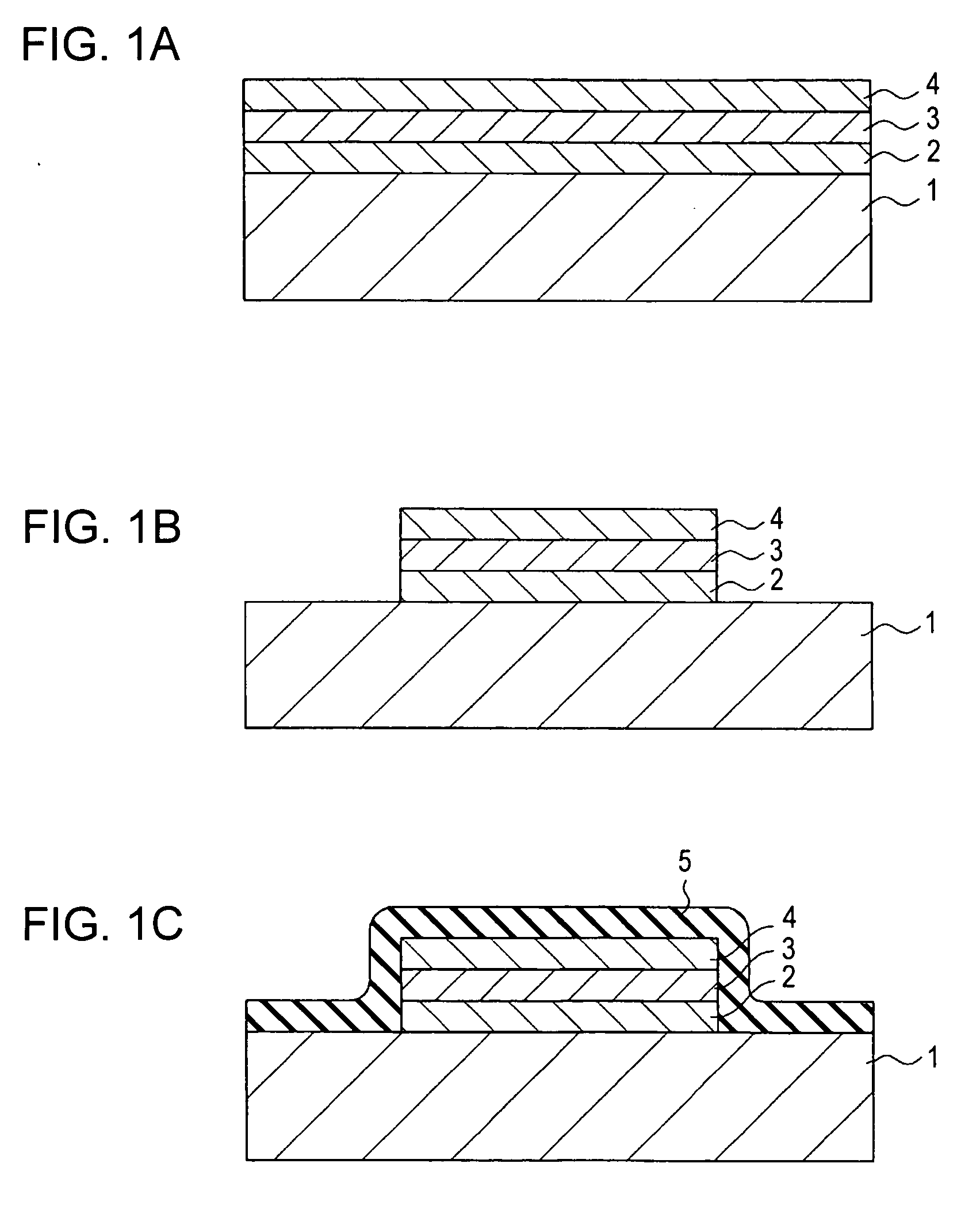
[0051] Hereinafter, a method of manufacturing a semiconductor device according to an embodiment of the invention will be described with reference to the accompanying drawings.

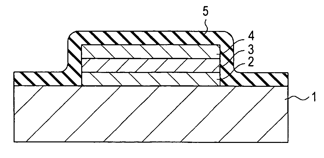
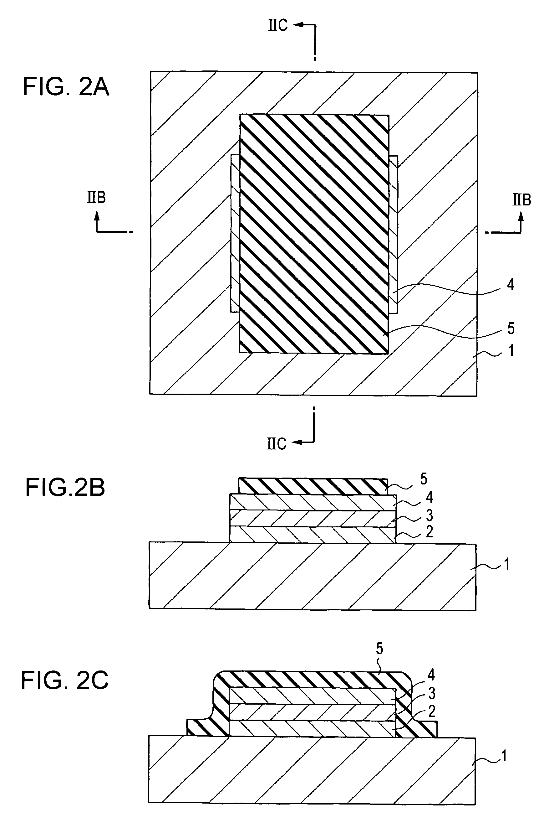
[0052]FIGS. 1A to 1C and 4A to 4C are cross-sectional views illustrating a method of manufacturing a semiconductor device according to a first embodiment of the invention. FIGS. 2A and 3A are plan views illustrating the method of manufacturing the semiconductor device according to the first embodiment of the invention. FIG. 2B is a cross-sectional view taken along the line IIB-IIB of FIG. 2A, and FIG. 2C is a cross-sectional view taken along the line IIC-IIC of FIG. 2A. FIG. 3B is a cross-sectional view taken along the line IIIB-IIIB of FIG. 3A, and FIG. 3C is a cross-sectional view taken along the line IIIC-IIIC of FIG. 3A.

[0053] Referring to FIG. 1A, a first semiconductor layer 2 and a second semiconductor layer 3 are sequentially formed on a semiconductor substrate 1 by performing epitaxial growth. The sem...


PUM


Abstract

A semiconductor substrate includes a semiconductor base substrate that has an oxide film selectively formed on a part thereof, the oxide film having a non-uniform thickness; and a semiconductor layer that is formed on the oxide film by epitaxial growth so as to have a non-uniform thickness.

Description

[0001] Applicant claims foreign priority to Japanese Application No. 2004-315334 filed on Oct. 29, 2004, which is hereby incorporated by reference in its entirety. BACKGROUND OF THE INVENTION [0002] 1. Technical Field [0003] The present invention relates to a semiconductor substrate, to a semiconductor device, to a method of manufacturing a semiconductor substrate, and to a method of manufacturing a semiconductor device. In particular, the invention relates to a technique suitably applicable to field effect transistors formed on an SOI (silicon on insulator) substrate. [0004] 2. Related Art [0005] Field effect transistors formed on an SOI substrate have drawn attention in terms of ease of element separation, latch-up free property, small source / drain junction capacitance, and so on. In particular, since a fully depleted SOI transistor has features, such as low power consumption, high-speed operation, and low-voltage driving, research for operating an SOI transistor in the fully depl...

Claims


Application Information

Patent Timeline
Patent Type & Authority Applications(United States)
IPC IPC(8): H01L27/10
CPCH01L29/66772H01L29/78612H01L29/78621H01L29/78696
Inventor HARA, TOSHIKI
Owner SEIKO EPSON CORP
Why Eureka
Try Eureka