
Multilayered barrier metal thin-films
a metal thin film, multi-layer technology, applied in the direction of coatings, basic electric elements, chemical vapor deposition coatings, etc., can solve the problems of film properties, conventional metal organic chemical vapor deposition (mocvd), and does not allow the manufacture of films having a smaller thickness, so as to improve the adhesion characteristics
- Summary
- Abstract
- Description
- Claims
- Application Information
AI Technical Summary
Benefits of technology
Problems solved by technology
Method used
Image

Examples
Embodiment Construction
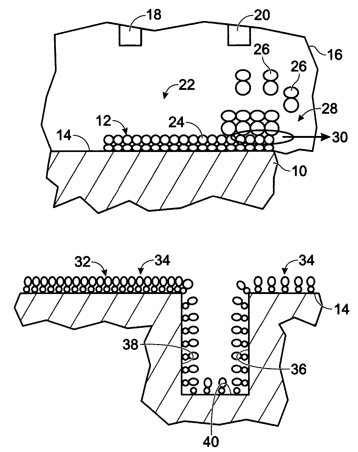
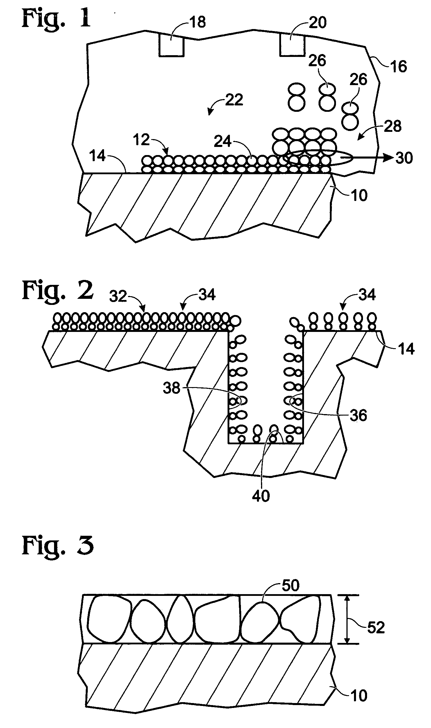
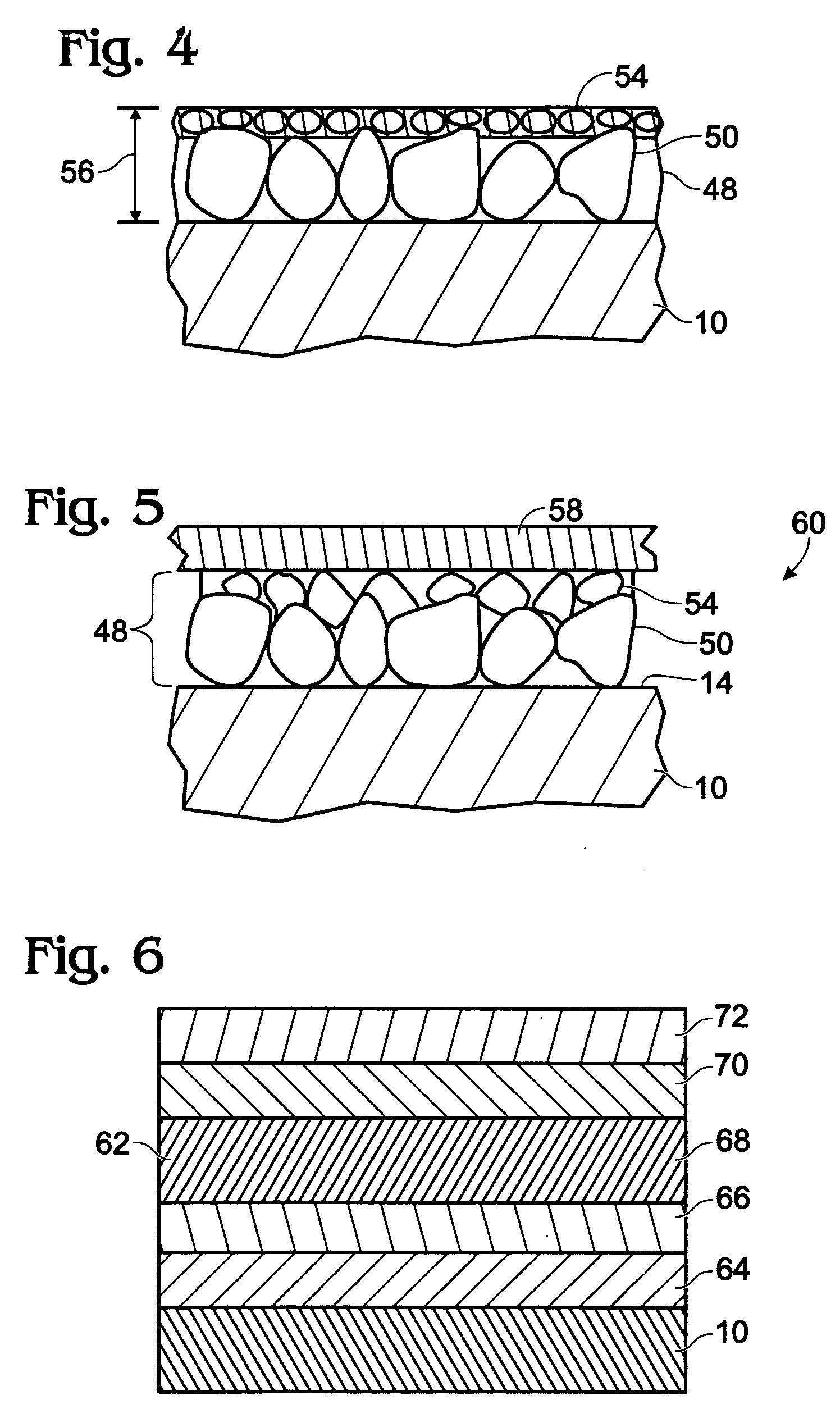
[0018] Atomic layer chemical vapor deposition (ALCVD) is an emerging technology that is being adopted in mainstream semiconductor research for eventual transfer to manufacturing. ALCVD uses fast operating valves to deliver individual reactants to a deposition chamber. Each reactant lays a mono-layer, i.e., an atomic layer, or several mono-layers, on the wafer structure through chemical adsorption and reacts with a previously deposited mono-layer species to form a desired compound. The as-formed compound will have a higher density than can be achieved by conventional CVD methods. The as-formed compound will also have excellent step coverage. By carefully selecting precursors, multi-layered or alternating layered barrier metal films are achievable. For example, alternating Tantalum Nitride / Silicon Nitride (TaN / SiN), Tantalum Nitride / Titanium Nitride (TaN / TiN) and Titanium Nitride / Silicon Nitride (TiN / SiN) thin films, or their combinations, are relatively easy to deposit using the ALCV...
PUM
| Property | Measurement | Unit |
|---|---|---|
| thickness | aaaaa | aaaaa |
| thickness | aaaaa | aaaaa |
| thickness | aaaaa | aaaaa |
Abstract
Description
Claims
Application Information