Method for forming a dual layer, low resistance metallization during the formation of a semiconductor device

a semiconductor device and dual layer technology, applied in the direction of semiconductor devices, semiconductor/solid-state device details, electrical equipment, etc., can solve problems such as difficult to achieve, and achieve the effects of low resistance, reduced cross-sectional area, and high resistance contacts

Inactive Publication Date: 2006-05-11
MICRON TECH INC
View PDF4 Cites 205 Cited by
  • Summary
  • Abstract
  • Description
  • Claims
  • Application Information

AI Technical Summary

Benefits of technology

[0007] The present invention provides a new method which reduces problems associated with the manufacture of semiconductor devices, particularl

Problems solved by technology

Such a damascene process requires polishing of a hard metal w

Method used


Image

  • Method for forming a dual layer, low resistance metallization during the formation of a semiconductor device
  • Method for forming a dual layer, low resistance metallization during the formation of a semiconductor device
  • Method for forming a dual layer, low resistance metallization during the formation of a semiconductor device

Examples


Embodiment Construction

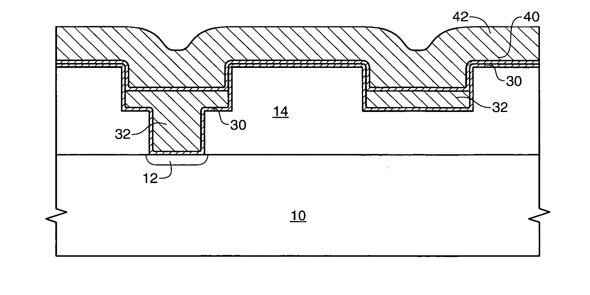
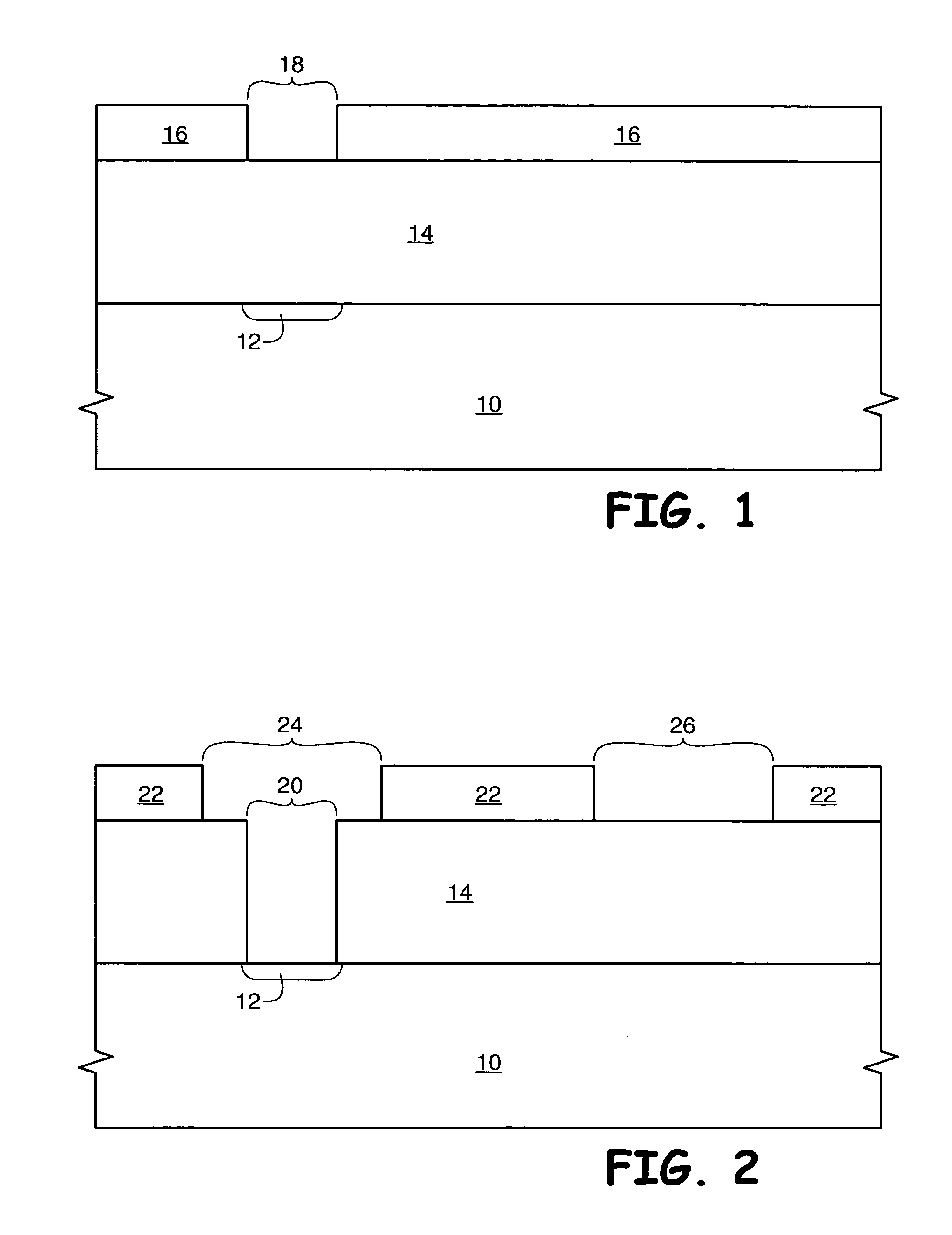
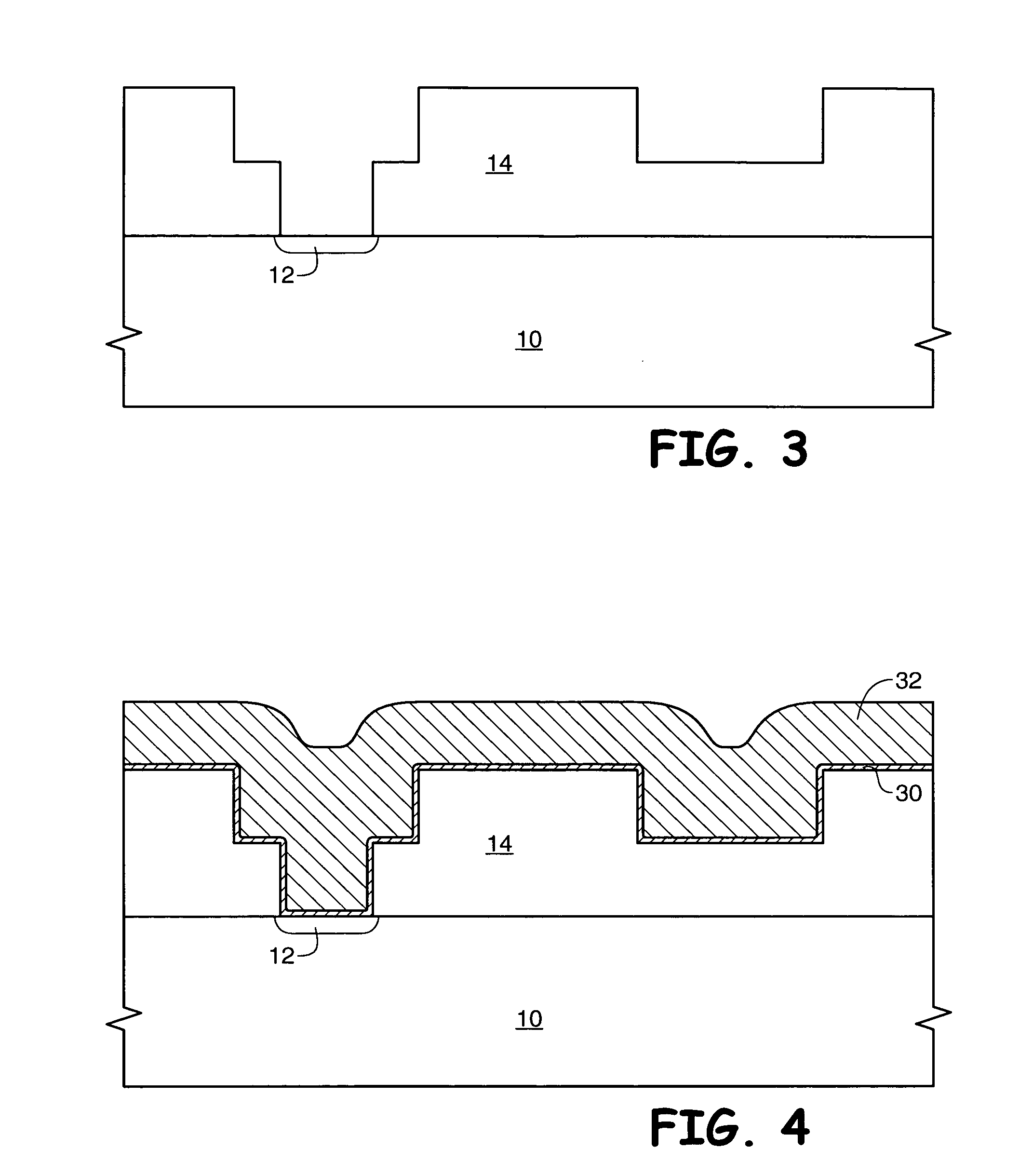
[0016] The term “wafer” is to be understood as a semiconductor-based material including silicon, silicon-on-insulator (SOI) or silicon-on-sapphire (SOS) technology, doped and undoped semiconductors, epitaxial layers of silicon supported by a base semiconductor foundation, and other semiconductor structures. Furthermore, when reference is made to a “wafer” in the following description, previous process steps may have been utilized to form regions or junctions in or over the base semiconductor structure or foundation. Additionally, when reference is made to a “substrate assembly” in the following description, the substrate assembly may include a wafer with layers including dielectrics and conductors, and features such as transistors, formed thereover, depending on the particular stage of processing. In addition, the semiconductor need not be silicon-based, but could be based on silicon-germanium, silicon-on-insulator, silicon-on-sapphire, germanium, or gallium arsenide, among others. ...


PUM


Abstract

A method for providing a highly reliable, low resistance interconnect comprises forming a trench in a dielectric layer, forming a first liner in the trench then forming a resilient layer such as a tungsten layer within the trench. The resilient layer is etched back to remove the layer from a horizontal portion of the dielectric outside the trench and to recess the layer within the trench. Next, a second liner and a copper layer are formed in the trench over the resilient layer. The copper layer and exposed portions of the two liners are polished or etched back to result in the interconnect. Variations to this embodiment are also described.

Description

FIELD OF THE INVENTION [0001] This invention relates to the field of semiconductor manufacture and, more particularly, to a conductive line comprising at least two metal layers and a liner, and a method for forming the conductive line. BACKGROUND OF THE INVENTION [0002] Many structures are required during the manufacture of a semiconductor device, such as conductive plugs, transistors, capacitors, and conductive lines. A common design goal of semiconductor engineers is to decrease the size of these features to increase the number of features which can be formed in a given area. Decreasing feature size results in decreased production costs and, ultimately, miniaturized electronic devices into which the semiconductor device is installed. [0003] Increasing electrical resistance is a concern with decreasing device feature size. For example, as the width of conductive lines decreases the resistance increases, especially with the relatively longer lines such as word lines in memory device...

Claims


Application Information

Patent Timeline
IPC IPC(8): H01L23/52H01L21/4763
CPCH01L21/76847H01L21/76877
Inventor RUSSELL, STEPHEN W.
Owner MICRON TECH INC
Why Eureka
Try Eureka