Method and a laser device for producing high optical power density

a laser device and optical power density technology, applied in the direction of lasers, semiconductor laser arrangements, instruments, etc., can solve the problems of increasing the size of the light source, the inability to increase the brightness of a single light source by passive optical elements, and the light power of a single semiconductor emitter is fairly limited, so as to achieve efficient utilization of spatial, wavelength and polarization multiplexing, and simplify or more effective cooling

Inactive Publication Date: 2006-05-11
KJELLBERG STIFTUNG
View PDF23 Cites 17 Cited by
  • Summary
  • Abstract
  • Description
  • Claims
  • Application Information

AI Technical Summary

Benefits of technology

[0023] The narrower than conventional structure of the laser bars according to the present invention provides a simplified or more effective cooling compared to the broad laser bars in prior art. The fact that the laser bars are narrow also involves that it is possible to avoid the prior art cumbersome and limiting narrowing optics of the light beam in the direction of the slow axis. This, in turn, enables very compact axial symmetrical structural solutions, which enable utilization of spatial, wavelength and polarisation multiplexing efficiently at the same time.
[0024] Hence, the solution of the invention enables increasing the power density of the radiation composed of different laser bars closer towards the theoretical maximum that would be obtained in an ideal situation in which the optical efficiency of different emitters could be combined without losses and directed to a desired point. Therefore, the solution of the invention makes it possible to achieve power densities that are higher than those of prior art, as well as a better combined beam quality.

Problems solved by technology

The brightness of a single light source cannot be increased by passive optical elements.
As for semiconductor lasers, the light power of a single semiconductor emitter is fairly limited, wherein in order to obtain a sufficient total light power a large number of single emitters are required.
Nevertheless, as the number of the emitters in a light source is thereby increasing, it is inevitable that also the size of the light source increases.
The power density can be increased, but since the solid angle of light grows in the same relation, the brightness cannot be increased with mere spatial multiplexing.
In practice it is very difficult to design and implement a structure that would combine a plurality of semiconducter laser beams in an efficient manner and simultaneously use wavelength, polarisation and spatial multiplexing.
The structure is simple, but a part of the light power is lost as reflection losses.
Furthermore, it is difficult to implement different multiplexing methods simultaneously using the referred method, wherein the maximum power density obtained is limited.
However, in practice waveguides often reduce the brightness of the light source in a significant manner.
This is due to the fact that a high fill factor cannot be achieved at the exit end of the waveguides.
The waveguides must have a sufficiently large light coupling end in order to collect all the light power, but often a part of the coupling surface is inefficient wherein the total brightness deteriorates.
Polarisation and wavelength multiplexing cannot be directly connected to the use of the waveguides either.
To maintain the laser brightness in the slow axis direction is perhaps the most common problem in combining bright diode laser beams, for which problem solutions are disclosed in a plurality of patent publications.
Nevertheless, such solutions are not advantageous in practice, as the exploitation level of the laser wafer will be poor because most of the wafer is composed of empty space between the emitters.
In addition, the physical space required by the narrowing and piling optics makes the combining of different multiplexing methods difficult.
Due to the diverging of the slow axis the light intended for different glass sheets is partly mixed and this part is lost.
In this method a plurality of cylindrical lenses, ball lenses and glass lenses are needed, which adds to the size of the structure and makes simultaneous utilization of different multiplexing methods difficult.
The structure of the device according to the method is, however, of “L” shape, which requires a large space.
As a result of this, combining the beams of a plurality of laser bars is not very advantageous.
Frequently, also problems related to the manufacturing technique of micromirrors are limiting factors.
However, small mirror structures integrated of glass bars are difficult to manufacture, and the laser bars cannot be brought close to each other in this solution either.
The structure is simple, but the laser bars cannot be brought close to each other, because the deflection must be carried out in the direction of the fast axis.
The above-described solutions facilitate the handling of the slow axis at the cost of more complicated structures and increased physical size of the technical solutions, which, in turn, makes the simultaneous usage of different multiplexing methods difficult and thereby limits the brightness and power density.

Method used


Image

  • Method and a laser device for producing high optical power density
  • Method and a laser device for producing high optical power density
  • Method and a laser device for producing high optical power density

Examples


embodiment

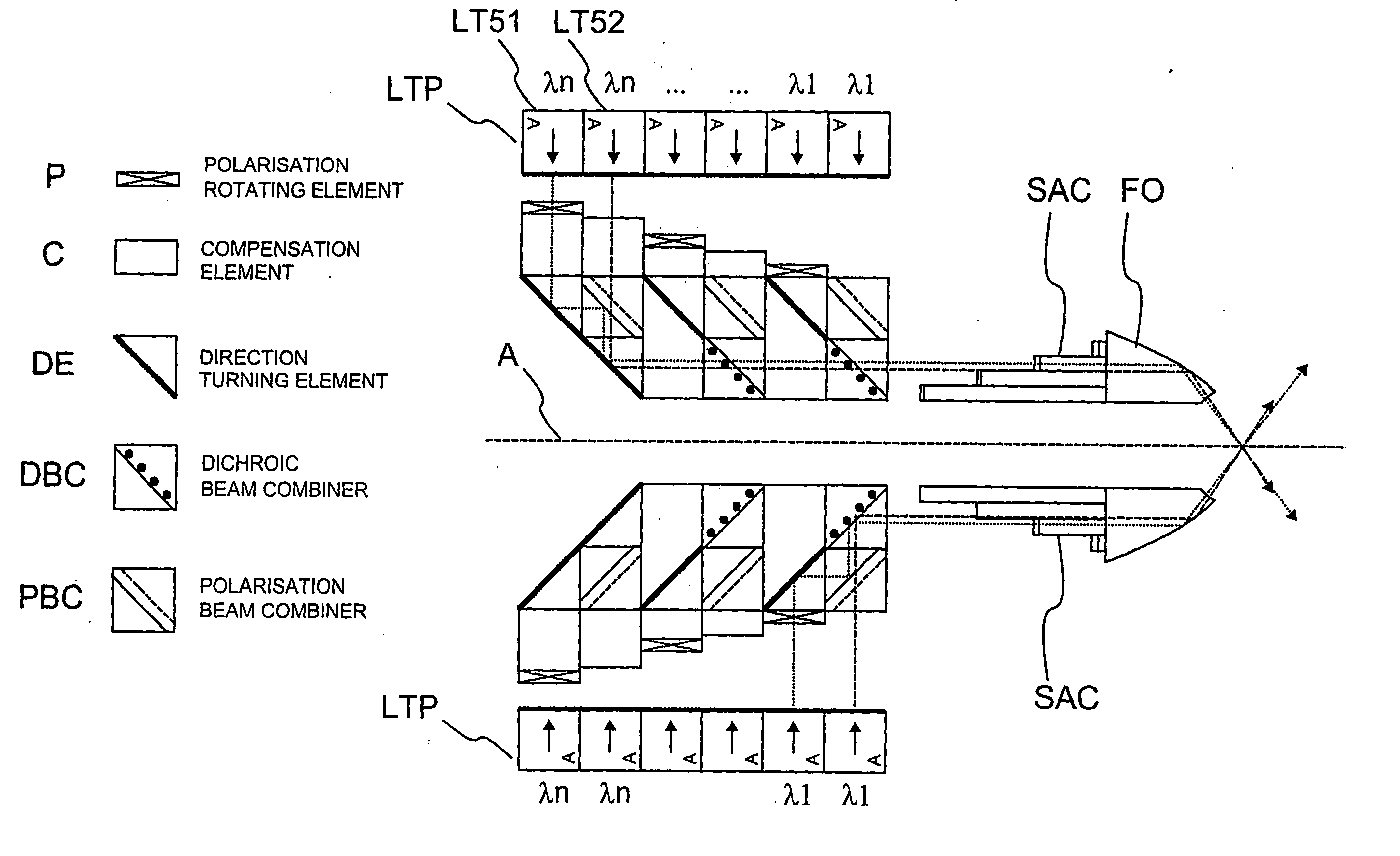
[0123] Embodiment According to FIG. 6

[0124]FIG. 6 describes one embodiment of the invention, in which all above-mentioned multiplexing methods are utilized simultaneously. In each sector laser the tower piles LTP61 and LTP62 manufactured of laser towers LT are positioned to two directions that are perpendicular against each other and said laser tower piles can be identical with each other. The laser tower piles LTP61 and LTP62 can be coupled in series for cooling, and they comprise suitable optical elements for compensation. The polarisation planes of the second laser tower pile LTP61 are turned 90°, whereafter the beams can be combined by using the polarisation beam combiner. The slow axis can be collimated by one steplike pile of lenses SAC after the beams have been combined. Another alternative is to provide each laser tower or laser tower pile with an individual collomation optics SAC of the slow axis.

[0125] Also in this solution the structure can be simplified in a manner allo...


PUM

PropertyMeasurementUnit
widthaaaaaaaaaa
angleaaaaaaaaaa
heightaaaaaaaaaa

Abstract

The invention relates to a method and laser device for producing a high optical power density by forming laser bars (LB) of diode lasers (E) in a manner that in a single laser bar (LB) the slow axes (x) of adjacent diode lasers (E) are positioned relative to each other in the same line and said diode lasers (E) emit substantially to the same direction (z), and radiation emitted by said plurality of laser bar (LB) is further collected to a combined and bright beam that is parallel with the optical axis (A). In accordance with the invention the laser bars (LB) are arranged in sectors relative to the optical axis (A) to an axial symmetrical structure in a manner that the direction of beams leaving from different sectors is turned (DE) in order to combine said beams. Preferred embodiments of the invention enable combination of efficient sector-by-sector radiation of laser bars (LB) using spatial, polarisation and/or wavelength multiplexing.

Description

[0001] The invention relates to a method according to the preamble of claim 1 for producing a large optical power density. The invention further relates to a laser device implementing the above-mentioned method in accordance with the preamble of the accompanying claim 17. BACKGROUND OF THE INVENTION [0002] Bright light produced by laser devices is today utilized in a multitude of different processes. Such processes include e.g. material marking, surface treatment, cutting and welding. High power lasers are applicable e.g. for handling of metal materials using the above-mentioned processes. Lasers are also widely applied for medical purposes and in various optical measurements. [0003] Since diode lasers based on semiconductors are developing, increasing the optical power obtained thereby and improving the beam quality, applications using compact semiconductor lasers have been strongly expanded for the above-mentioned application areas, which have traditionally been using larger size ...

Claims


Application Information

Patent Timeline
Patent Type & Authority Applications(United States)
IPC IPC(8): H01S3/13B23K26/06G02B27/10H01S5/40
CPCB23K26/0604B23K26/0613G02B27/145H01S5/4012H01S5/4025H01S5/4087G02B19/0057G02B19/0028
Inventor ALAHAUTALA, TAITOLASSILA, ERKKI
Owner KJELLBERG STIFTUNG
Why Eureka
Try Eureka