Light emitting element

a technology of light-emitting elements and components, which is applied in semiconductor lasers, semiconductor/solid-state device details, lighting and heating apparatus, etc., can solve the problems of increasing the volume of heat generated, increasing the number of processes, and enlarged portions protruding out of the case, so as to achieve less resin leakage and facilitate fabrication.

Inactive Publication Date: 2006-05-25
SANYO ELECTRIC CO LTD +1
View PDF5 Cites 27 Cited by
  • Summary
  • Abstract
  • Description
  • Claims
  • Application Information

AI Technical Summary

Benefits of technology

[0019] According to a thirteenth aspect of the invention, in the light emitting element structured as described above, a concave portion for receiving a lead is formed on the outer bottom surface of the case, and portions of the first and second leads that p...

Problems solved by technology

The increase in the power exerted by a semiconductor laser results in an increase in the volume of heat generated.
The increase in the temperature of a light emitting element causes problems such as deformation or discoloration of the case that encloses the semiconductor laser, requiring more effective measures against heat.
Simply increasing the area of the lead frame, however, may result...

Method used


Image

  • Light emitting element
  • Light emitting element
  • Light emitting element

Examples


first embodiment

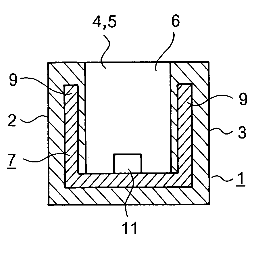
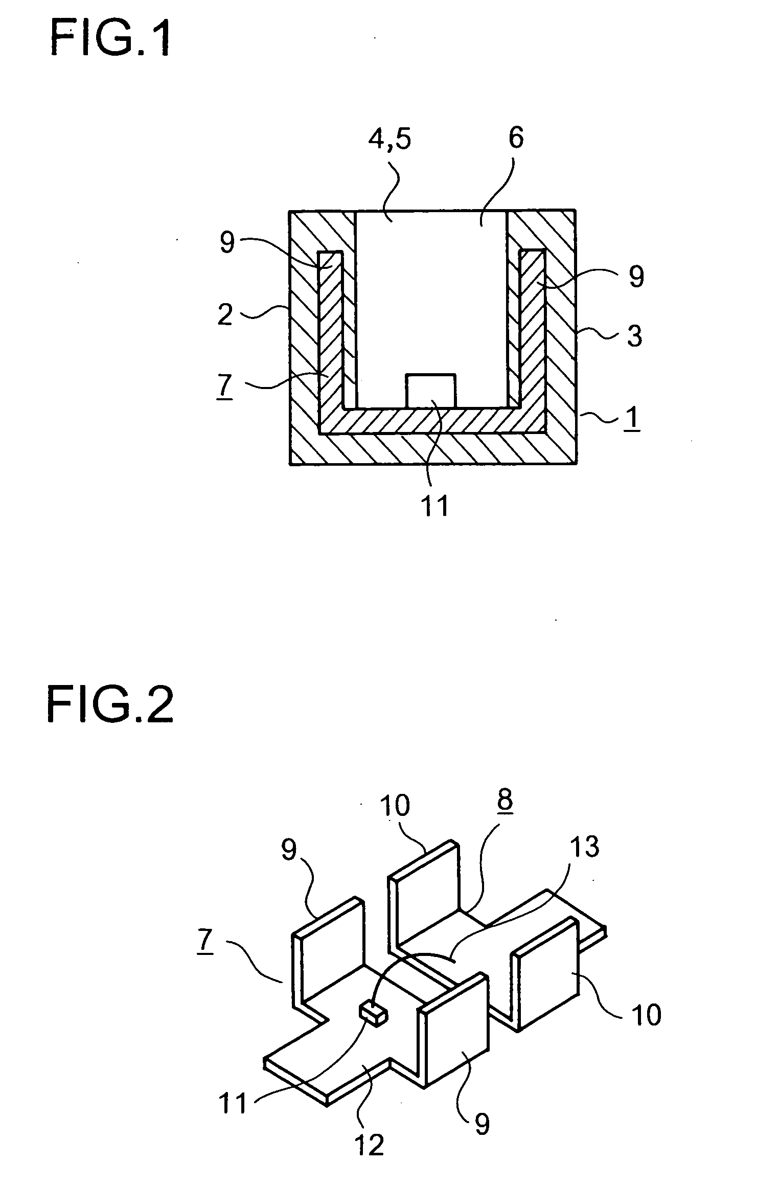
[0037]FIGS. 1 and 2 show the present invention. FIG. 1 is a cross section of a light emitting element. FIG. 2 is a perspective view of lead frames used in the light emitting element of FIG. 1.

[0038] The light emitting element includes a box-shaped case 1 formed out of an insulating material, such as epoxy resin. The case 1 has a hollow portion 6 formed inside it surrounded by the four side walls 2, 3, 4, and 5 thereof so as to be open at the top. To the case 1 are fixed a first lead frame 7 and a second lead frame 8. The first and second lead frames 7 and 8 are formed out of a conductive material such as copper, iron, or aluminum, and are integrally molded with the case 1.

[0039] As observed in FIG. 2, the first and second lead frames 7 and 8 are mutually symmetrical in shape. Each of the lead frames has two edges bent upward, thereby forming rise portions 9 on the first lead frame 7 and rise portions 10 on the second lead frame 8. When the case 1 is molded, the rise portions 9 and ...

second embodiment

[0045]FIG. 4 shows the present invention. FIG. 4 is a cross section of a light emitting element.

[0046] In the second embodiment, the light emitting element includes a first lead frame 7 and a second lead frame 8 built with the same structure as those shown in FIGS. 2 and 3. The first and second lead frames 7 and 8, however, have rise portions 9 and 10, respectively, which are arranged not inside but along and in close contact with the inner surfaces of the side walls 2 and 3. Thus, the rise portions 9 and 10 directly face a light emitting chip 11, thereby permitting the heat emitted by the light emitting chip 11 to be quickly dissipated.

third embodiment

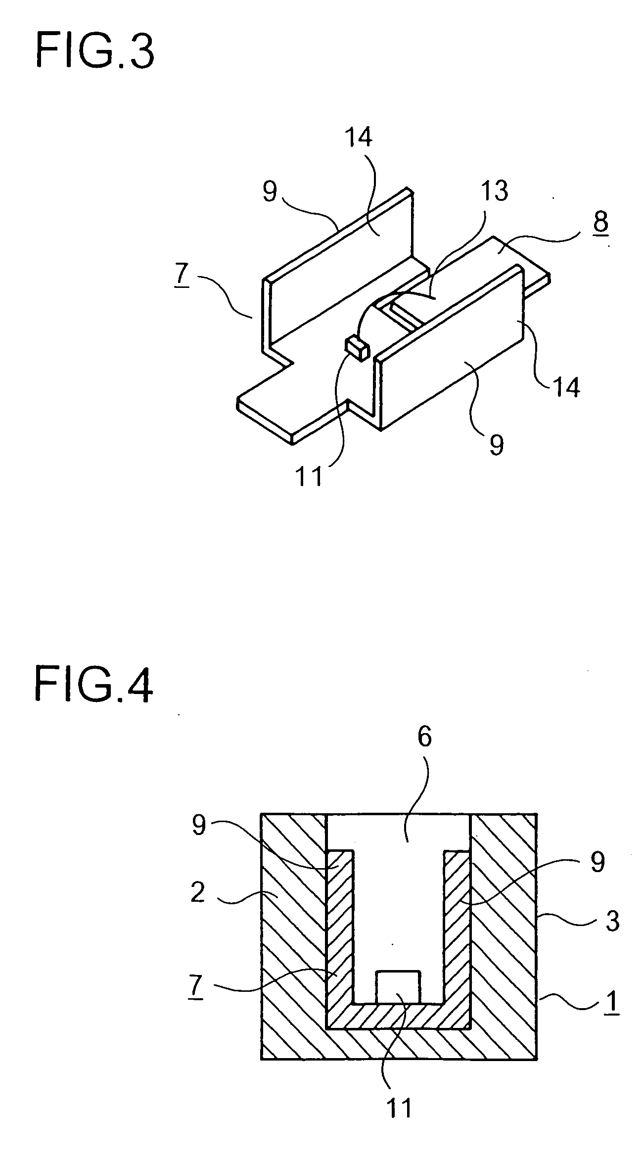
[0047]FIGS. 5 and 6 show the present invention. FIG. 5 is a cross section of a light emitting element. FIG. 6 is a perspective view of lead frames used in the light emitting element of FIG. 5.

[0048] In the third embodiment, a first lead frame 7 and a second lead frame 8 are mutually symmetrical in shape and structured in the following manner. Specifically, the first lead frame 7 includes: a bottom portion 12; rise portions 9 formed by bending upward the both side edges of the bottom portion 12; a rise portion 20 formed by bending upward an end edge 18 orthogonal to the side edges; and a lead portion 16 protruding from the rise portion 20. The second lead frame 8 includes: a bottom portion 15; rise portions 10 formed by bending upward the both side edges of the bottom portion 15; a rise portion 21 formed by bending upward an end edge 19 orthogonal to the side edges; and a lead portion 17 protruding from the rise portion 21.

[0049] The rise portions 9 and 20 of the first lead frame 7 ...


PUM


Abstract

A light emitting element includes: a box-shaped case formed by an insulation material and having a space inside; a lead frame formed by a conductive material and fixed to the case; and a light emitting chip fixed to the lead frame. On the lead frame, a rise portion is formed in a side wall of the case or along the inner surface of the side wall. The lead frame has a first lead frame fixing the light emitting chip and a second lead frame connected to the light emitting chip by the wire bonding. At least on the first lead frame, a rise portion is formed.

Description

TECHNICAL FIELD [0001] The present invention relates to a light emitting element that is built by combining together a light emitting chip and a lead frame. BACKGROUND ART [0002] There is one type of light emitting element called a frame laser. The frame laser is built by fixing a pair of lead frames formed out of a conductive material in a case formed out of an insulating material, with a semiconductor laser element fixed on one of the lead frames and connected by wire bonding to the other lead frame. Japanese Patent Application Laid-open No. H3-188692 discloses an example of a frame laser. Japanese Patent Application Laid-open No. 2003-152228 discloses an example of a light emitting element having a light emitting diode fixed on a lead frame. [0003] Semiconductor lasers are widely used in writing data onto optical recording media or reading data therefrom. Due to a recent trend toward large capacity optical discs, the volume of data to be read and written has significantly increas...

Claims


Application Information

Patent Timeline
IPC IPC(8): F21V29/00H01L23/495H01L23/498H01L33/48H01L33/60H01L33/62H01S5/0232H01S5/024
CPCH01L23/49861H01L33/483H01L33/60H01L33/62H01L2224/48091H01L2224/48247H01S5/02244H01S5/024H01L2924/00014H01L2924/12041H01S5/0231H01S5/0232
Inventor MATSUMOTO, AKIHISAMOTOIKE, TATSUYANAKAHARA, TOSHINORI
Owner SANYO ELECTRIC CO LTD
Why Eureka
Try Eureka