CR oscillation circuit

a technology of oscillation circuit and oscillation frequency, which is applied in the direction of pulse generator, pulse technique, instruments, etc., can solve the problems of display flicker, increase in semiconductor integrated circuit cost, etc., and achieve the effect of suppressing clock frequency variation

Inactive Publication Date: 2006-05-25
COLLABO INNOVATIONS INC
View PDF6 Cites 5 Cited by
  • Summary
  • Abstract
  • Description
  • Claims
  • Application Information

AI Technical Summary

Benefits of technology

[0011] In view of the above, an objective of the present invention is to suppress

Problems solved by technology

Thus, the cost of the semiconductor integrated circuit increases

Method used


Image

  • CR oscillation circuit
  • CR oscillation circuit
  • CR oscillation circuit

Examples


embodiment 1

[0041]

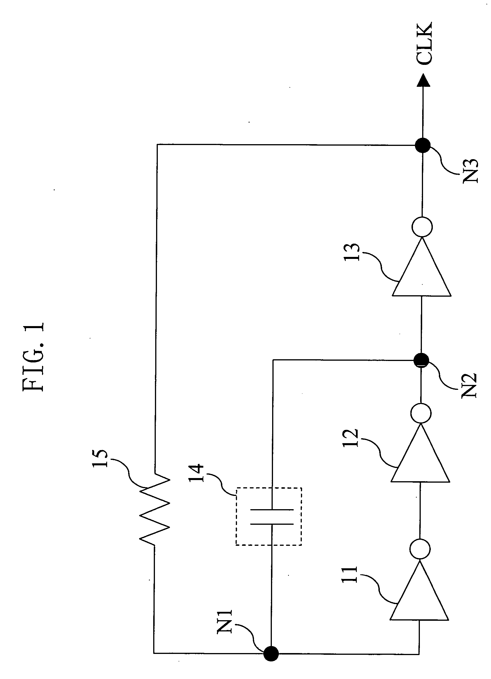
[0042]FIG. 1 is a circuit diagram of a CR oscillation circuit according to embodiment 1 of the present invention. This circuit includes inverters 11, 12 and 13, a capacitive element 14, and a resistive element 15. The inverters 11, 12 and 13 are connected in series between a node N1 and a node N3. The capacitive element 14 is connected between the node N1 and a node N2, which is a connection node between the inverter 12 and the inverter 13, in parallel with the inverters 11 and 12. The resistive element 15 is connected between the node N1 and the node N3 in parallel with the inverters 11, 12 and 13. The resistive element 15 is, for example, a polysilicon resistance.

[0043] In the CR oscillation circuit having such a structure, it has been generally known that the frequency of clock CLK output therefrom can be calculated by the formula of “1 / (2.2×C×R)” where C is the capacitance value of the capacitive element 14 and R is the resistance value of the resistive element 15. It sho...

embodiment 2

[0070]

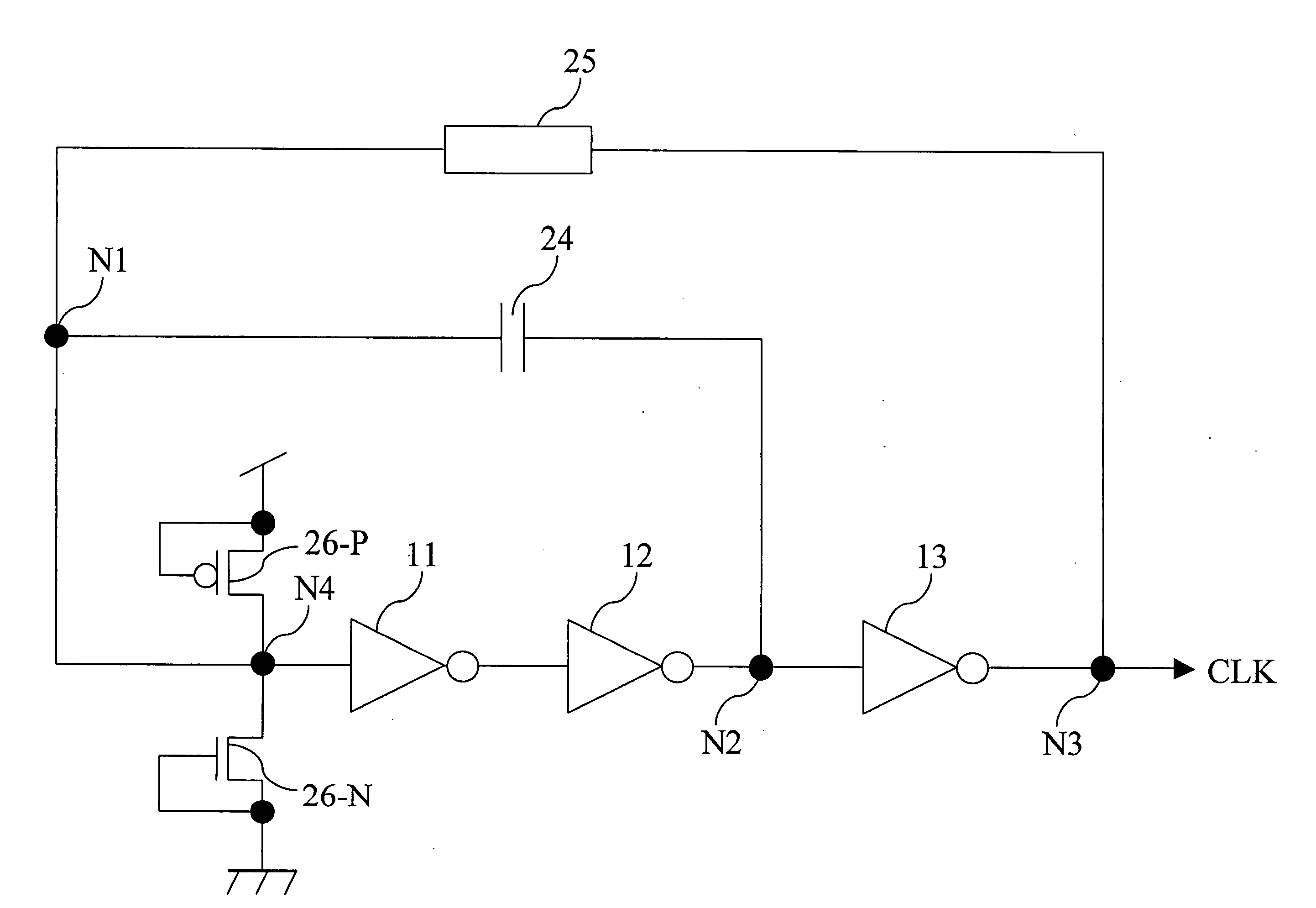
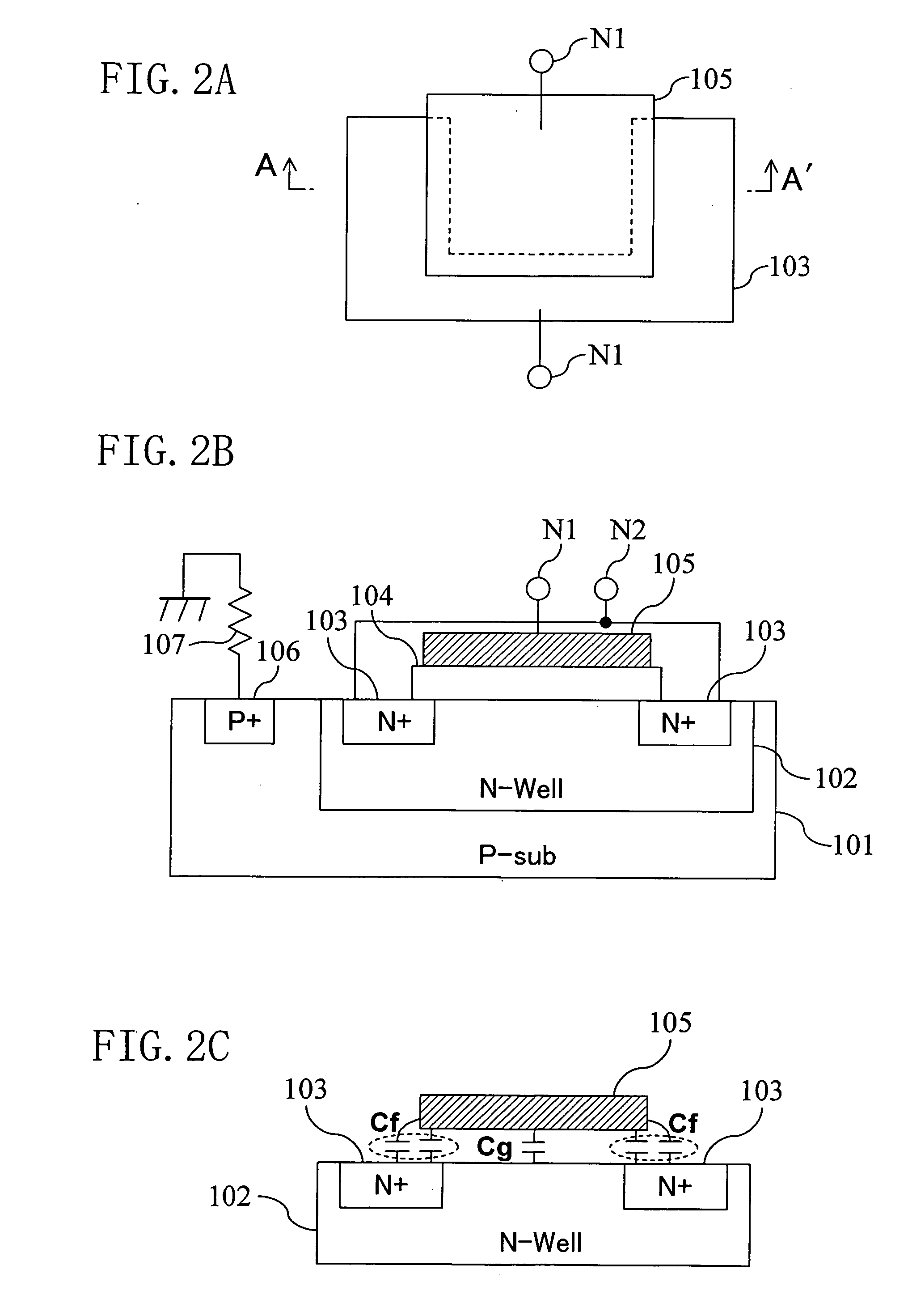
[0071]FIG. 6 shows the structure of a CR oscillation circuit according to embodiment 2 of the present invention. The CR oscillation circuit of embodiment 2 includes a capacitive element 24 and a resistive element 25 in place of the capacitive element 14 and the resistive element 15 of FIG. 1. The CR oscillation circuit further includes a P-type MOS transistor 26-P and an N-type MOS transistor 26-N. The other parts of the structure are the same as those of FIG. 1. The capacitive element 24 may be, for example, an interlayer capacitance, such as an interpolysilicon capacitance or intermetal capacitance, or may alternatively be the capacitive element (gate oxide film capacitance) shown in FIG. 2, FIG. 4 or FIG. 5. The P-type MOS transistor 26-P is connected between a node N4 and a power supply node, and the source and gate of the P-type MOS transistor 26-P are connected to each other. The N-type MOS transistor 26-N is connected between the node N4 and a ground node, and the sourc...


PUM


Abstract

A CR oscillation circuit comprises first and second logic elements, a capacitive element, and a resistive element. The first logic element is connected between a first node and a second node. The second logic element is connected between the second node and a third node. The capacitive element is connected between the first node and the second node. The resistive element is connected between the first node and the third node. The capacitive element includes a well, a diffusion layer, a gate electrode and a gate oxide film. The capacitive element has a voltage-dependence characteristic such that its capacitance value varies according to the variation in a supply voltage. The capacitance value of the capacitive element decreases when the on-resistance of the first and second logic elements increases according to the variation in the supply voltage.

Description

CROSS-REFERENCE TO RELATED APPLICATIONS [0001] This application claims priority under 35 U.S.C. § 119(a) on Japanese Patent Application No. 2004-326221 filed on Nov. 10, 2004 and Japanese Patent Application No. 2005-280419 filed on Sep. 27, 2005, the entire contents of which are hereby incorporated by reference. BACKGROUND OF THE INVENTION [0002] 1. Field of the Invention [0003] The present invention relates to a CR oscillation circuit which generates a clock having a frequency determined according to the resistance value and capacitance value. [0004] 2. Description of the Prior Art [0005]FIG. 12 shows a structure of a conventional CR oscillation circuit. The CR oscillation circuit includes inverters 91, 92 and 93, a capacitive element 94, and a resistive element 95. This circuit outputs clock CLK which has a frequency determined according to a product of the capacitance value of the capacitive element 94 and the resistance value of the resistive element 95 (see, for example, Japane...

Claims


Application Information

Patent Timeline
IPC IPC(8): H03B5/20
CPCH03K3/03
Inventor NISHI, KAZUYOSHITAKIGUCHI, JUNJI
Owner COLLABO INNOVATIONS INC
Why Eureka
Try Eureka