Integrated circuit including silicon wafer with annealed glass paste

a silicon wafer and integrated circuit technology, applied in the field of integrated circuits, can solve the problems of high cost, large bulky size, inconvenient operation, etc., and achieve the effect of low dielectric loss

Inactive Publication Date: 2006-06-01
MARVELL WORLD TRADE LTD
View PDF96 Cites 34 Cited by
  • Summary
  • Abstract
  • Description
  • Claims
  • Application Information

AI Technical Summary

Benefits of technology

[0025] An integrated circuit package comprises an integrated circuit that comprises temperature sensing means for sensing a temperature of the integrated circuit. Storing means stores data relating to oscillator calibrations and for selecting one of the oscillator calibrations as a function of the sensed temperature. Oscillating means generates a reference signal having a frequency that is based on the selected one of the oscillator calibrations. Packaging means encases at least part of the integrated circuit and having a low dielectric loss.
[0026] In other features, the packaging means includes at least one material selected from a group consisting of polychlorotrifluoroethylene, fluorinated ethylene propylene copolymer, perfluoroalkoxy, and a copolymer of ethylene and tetrafluoroethylene. The packaging means includes a low dielectric loss plastic.
[0027] An integrated circuit package comprises an integrated circuit that comprises oscillating means for generating a reference signal having a frequency that is based on one of a plurality of oscillator calibrations settings and packaging means for encasing at least part of the integrated circuit and having a low dielectric loss.
[0028] In other features, the integrated circuit further comprises temperature sensing means for sensing a temperature of the integrated circuit. Storing means stores oscillator calibration data. The packaging means includes at least one material selected from a group consisting of polychlorotrifluoroethylene, fluorinated ethylene propylene copolymer, perfluoroalkoxy, and a copolymer of ethylene and tetrafluoroethylene. The packaging means includes a low dielectric loss plastic.

Problems solved by technology

However, crystal oscillators have several inherent disadvantages including large bulky size, fragility, and high cost.
In addition, the size and cost of crystal oscillators is related to the resonant frequency so that as the frequency increases, the size decreases, and the cost and fragility may rapidly increase.
As the size of electronic devices continues to decrease, the use of crystal oscillators becomes more problematic due to the size, fragility, and cost limitations.
Semiconductor oscillators have been a poor alternative to crystal oscillators and are generally unsuitable for use as a precision frequency reference due to excessive variation in the oscillating frequency, especially with changes in temperature.

Method used


Image

  • Integrated circuit including silicon wafer with annealed glass paste
  • Integrated circuit including silicon wafer with annealed glass paste
  • Integrated circuit including silicon wafer with annealed glass paste

Examples


Embodiment Construction

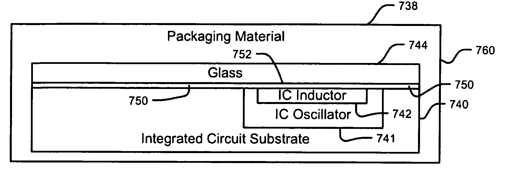
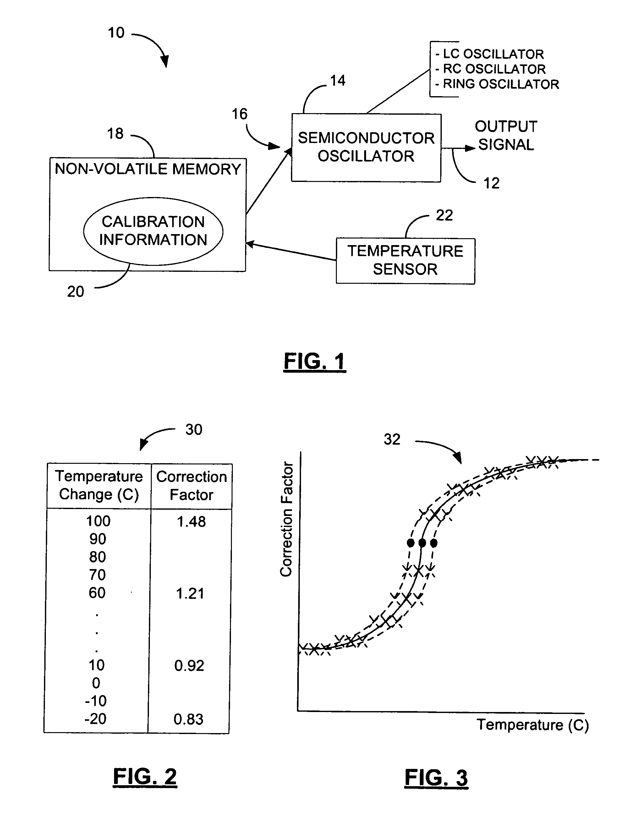
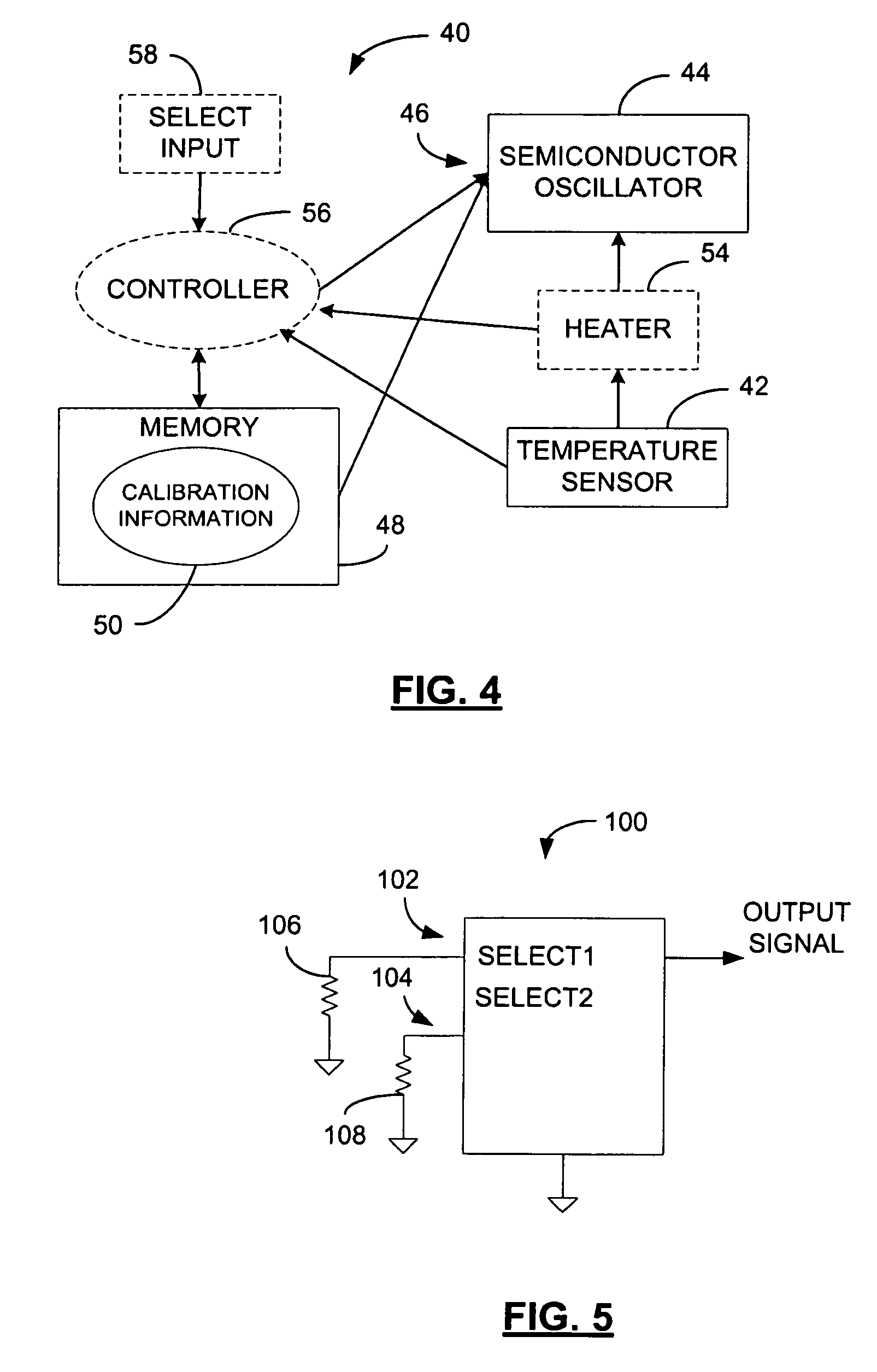
[0096]FIG. 1 shows an aspect of a crystal oscillator emulator 10 for generating an output signal 12 having a precise frequency. The crystal oscillator emulator 10 may be constructed on a single semiconductor die using any process including a Complementary-Metal-Oxide-Semiconductor (CMOS) process.

[0097] The crystal oscillator emulator 10 may include a semiconductor oscillator 14 to generate the output signal 12. Any type of semiconductor oscillator may be used including LC oscillators, RC oscillators, and ring oscillators. The semiconductor oscillator 12 includes a control input 16 to vary the frequency of the output signal. The control input 16 may be any electrical input that effects a controlled change in the output signal frequency such as the supply voltage of a ring oscillator and a voltage input to a varactor of an LC oscillator.

[0098] A non-volatile memory 18 includes calibration information 20 for controlling the output signal frequency as a function of temperature. Any ty...


PUM


Abstract

An integrated circuit (IC) package comprises an IC wafer and an annealed glass paste (AGP) layer that is arranged adjacent to the IC wafer. A molding material encapsulates at least part of the IC wafer and the AGP layer. The AGP layer is arranged on at least one side of the IC wafer. The AGP layer is arranged on a plurality of disjoint areas on at least one side of the IC wafer. A layer of a conductive material is arranged on a portion of the AGP layer.

Description

CROSS-REFERENCE TO RELATED APPLICATIONS [0001] This application claims the benefit of U.S. Provisional Application Nos. 60 / 714,454, filed on Sep. 6, 2005, and 60 / 730,568, filed on Oct. 27, 2005, and is a continuation-in-part of U.S. patent application Ser. No. 10 / 892,709, filed on Jul. 16, 2004, which is a continuation in part of U.S. patent application Ser. No. 10 / 272,247, filed on Oct. 15, 2002, the contents of which are hereby incorporated by reference in their entirety.TECHNICAL FIELD [0002] This invention relates to integrated circuits, and more particularly to integrated circuits with annealed glass paste arranged on a silicon wafer. BACKGROUND [0003] Precision frequency references are required in many types of electronic devices such as cellular phones and other handheld devices. Crystal oscillators are typically used to provide the precision frequency reference in these electronic devices. However, crystal oscillators have several inherent disadvantages including large bulky...

Claims


Application Information

Patent Timeline
Patent Type & Authority Applications(United States)
IPC IPC(8): H01L23/58
CPCB82Y10/00G11C7/04G11C7/22G11C7/222G11C29/028G11C2029/5002G11C2207/2254H01L23/315H01L23/34H01L2924/01046H01L2924/16235H01L2924/166H01L2924/19041H01L2924/30107H01L2924/3011H03L1/026H03L7/197H03L7/1976H01L24/48H01L24/49H01L2224/48227H01L2224/49175H01L2924/00H01L2924/10253H01L2224/05553H01L2924/00014H01L2924/14H01L2924/181H01L2924/00012H01L2224/45099H01L2224/45015H01L2924/207
Inventor SUTARDJA, SEHAT
Owner MARVELL WORLD TRADE LTD
Why Eureka
Try Eureka