Micro oscillating element

a technology of micro-oscillating elements and mirror surfaces, applied in the direction of optical elements, generators/motors, instruments, etc., can solve the problems of difficult to achieve a high degree of flatness on a mirror surface with a large surface area, thin mirror surface that is ultimately formed, and easy buckles

Inactive Publication Date: 2006-06-08
FUJITSU LTD
View PDF9 Cites 25 Cited by
  • Summary
  • Abstract
  • Description
  • Claims
  • Application Information

AI Technical Summary

Benefits of technology

[0023] In a preferred aspect, the micro oscillating element of the present invention may further comprise a third comb-tooth electrode and a fourth comb-tooth electrode cooperating with the third comb-tooth electrode for causing the oscillation section to oscillate. The third comb-tooth electrode may comprise a plurality of third electrode teeth that extend from the arm section in a direction intersecting the arm section, and that are spaced from each other in a longitudinal direction of the arm section. The fourth comb-tooth electrode may comprise a plurality of fourth electrode teeth that extend from the frame in a direction intersecting the arm section. In this case, the fourth comb-tooth electrode may be electrically separated from the second comb-tooth ele...

Problems solved by technology

However, with surface micromachining technology, the mirror surface that is ultimately formed is thin, and therefore buckles easily.
Accordingly, it is difficult to achieve a high degree of flatness on a mirror surface with a large surface area.
However, shrinking the length L61 cannot easily be compatible with maintaining the driving force enough to oscillate the mirror supporting portion 61.
However, reducing the width d1 and increasing the length d3 of the electrode ...

Method used


Image

  • Micro oscillating element
  • Micro oscillating element
  • Micro oscillating element

Examples


first embodiment

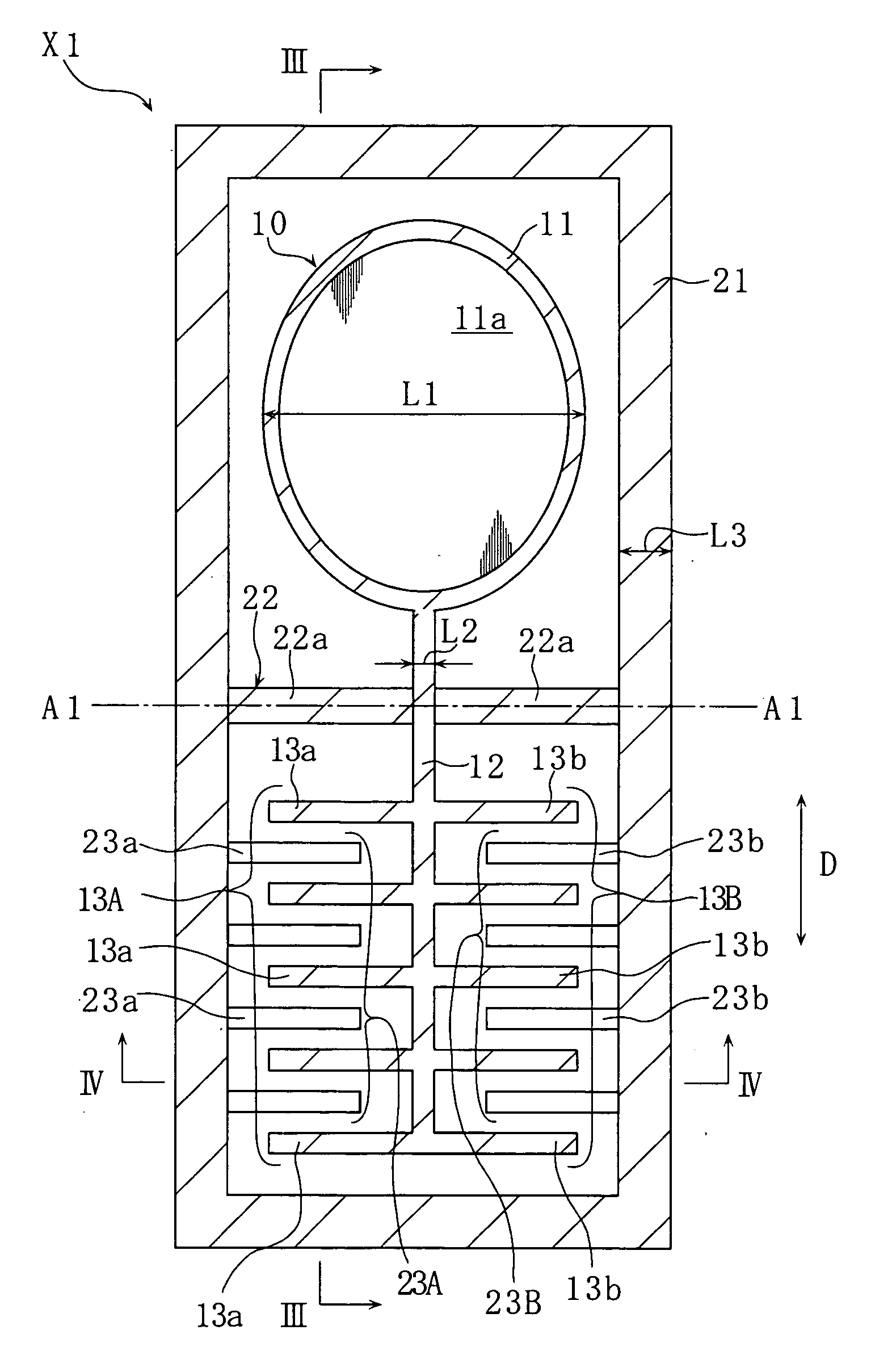
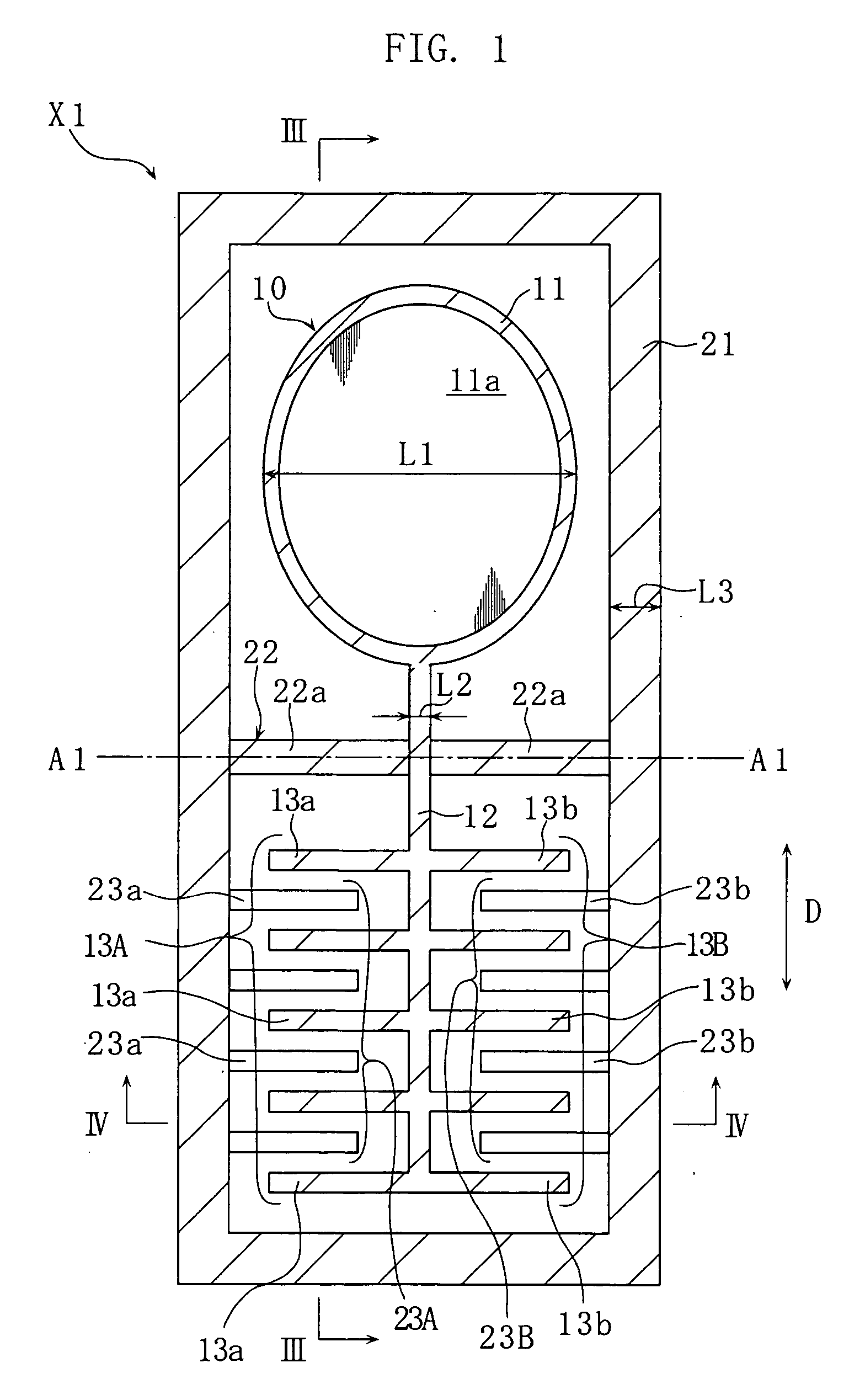
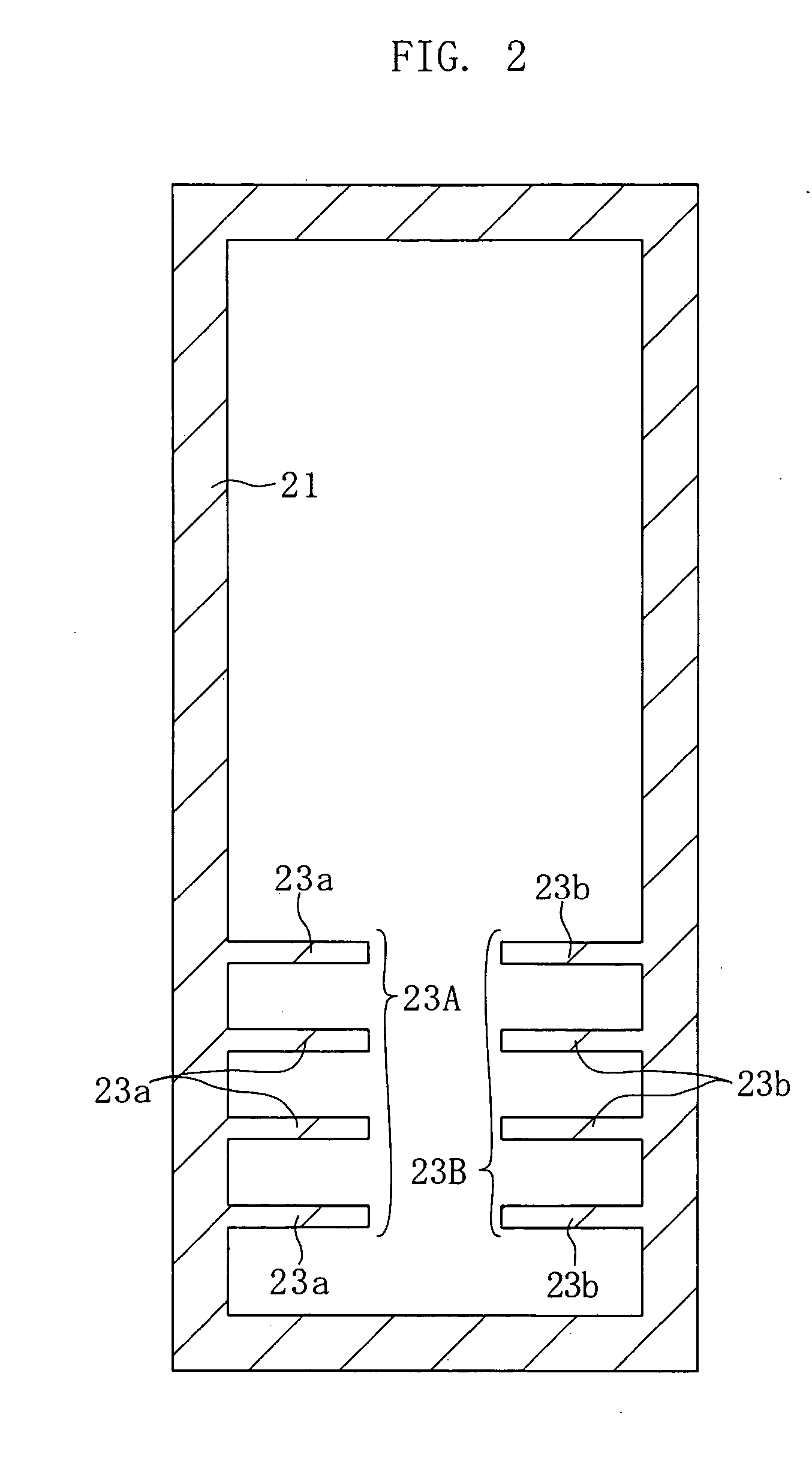
[0059] FIGS. 1 to 4 show a micromirror element X1 according to the present invention. FIG. 1 is a plan view of the micromirror element X1, FIG. 2 is a partial plan view of the micromirror element X1, and FIGS. 3 and 4 are sectional views along a line III-III and a line IV-IV respectively.

[0060] The micromirror element X1 comprises an oscillation section 10, a frame 21, a torsional joining section 22, and comb-tooth electrodes 23A, 23B, and is manufactured using bulk micromachining technology, such as MEMS technology, by machining a material substrate, which is a so-called SOI (silicon on insulator) substrate. The material substrate has a laminated structure constituted of a first silicon layer and second silicon layer, and an insulation layer provided between the silicon layers. Each silicon layer is provided with a predetermined conductivity by means of impurity doping. The aforementioned various regions of the micromirror element X1 are mainly formed on the first silicon layer and...

second embodiment

[0100] FIGS. 15 to 18 show a micromirror element X2 pertaining to the present invention. FIG. 15 is a plan view of the micromirror element X2, FIG. 16 is a partial plan view of the micromirror element X2, and FIGS. 17 and 18 are sectional views along a line XVII-XVII and a line XVIII-XVIII of FIG. 15, respectively.

[0101] The micromirror element X2 comprises an oscillation section 10, a frame 24, a torsional joining section 22, and comb-tooth electrodes 23A, 23B. The micromirror element X2 differs from the micromirror element X1 in comprising the frame 24 instead of the frame 21. Further, the micromirror element X2 is manufactured by machining a material substrate, which is an SOI substrate, using the MEMS technology described above in relation to the micromirror element X1. The material substrate has a laminated structure comprising a first silicon layer, a second silicon layer, and an insulation layer between the silicon layers, each silicon layer being provided with a predetermine...

third embodiment

[0110] FIGS. 19 to 23 show a micromirror element X3 according to the present invention. FIG. 19 is a plan view of the micromirror element X3, FIG. 20 is a partial plan view of the micromirror element X3, and FIGS. 21 to 23 are sectional views along a line XXI-XXI, a line XXII-XXII, and a line XXIII-XXIII in FIG. 19, respectively.

[0111] The micromirror element X3 comprises an oscillation section 10′, a frame 25, a torsional joining section 22, and comb-tooth electrodes 23A, 23B. The micromirror element X3 differs from the micromirror element X1 in comprising the oscillation section 10′ in place of the oscillation section 10, and in comprising the frame 25 in place of the frame 21. Further, the micromirror element X3 is manufactured by machining a material substrate, which is an SOI substrate, using the MEMS technology described above in relation to the micromirror element X1. The material substrate has a laminated structure comprising a first silicon layer, a second silicon layer, an...


PUM


Abstract

A micro oscillating element includes a frame and an oscillation section connected to the frame via a torsional joining section. The oscillation section includes a movable functional section, an arm section and a first comb-tooth electrode. The arm section extends from the functional section. The first comb-tooth electrode includes first electrode teeth extending from the arm section in a direction intersecting the arm section. The micro oscillating element further includes a second comb-tooth electrode to cooperate with the first comb-tooth electrode for causing the oscillation section to oscillate about an oscillation axis defined by the torsional joining section. The second comb-tooth electrode includes second electrode teeth extending from the frame in a direction intersecting the arm section.

Description

BACKGROUND OF THE INVENTION [0001] 1. Field of the Invention [0002] The present invention generally relates to a micro oscillating element having an oscillation section capable of rotary displacement. In particular, the present invention relates to a micromirror element, an acceleration sensor, an angular velocity sensor, and a vibration element, for example. [0003] 2. Description of the Related Art [0004] In recent years, elements having a microstructure formed by micromachining technology have been put to practical use in various technological fields. In the field of optical communication technology, for example, minute micromirror elements having a light reflecting function are gaining attention. [0005] In optical communication, optical signals are transmitted using optical fiber as a medium, and an optical switching device is typically used to switch the transmission path of the optical signal from one fiber to another fiber. To achieve favorable optical communication, the chara...

Claims


Application Information

Patent Timeline
IPC IPC(8): G02B26/08G02B26/00H02N1/00B81B3/00
CPCG02B26/0841H02N1/008B81C1/00142G02B26/0833G02B26/085B81B2203/0154Y10S359/904
Inventor KOUMA, NORINAOTSUBOI, OSAMUSONEDA, HIROMITSUUEDA, SATOSHISAWAKI, IPPEI
Owner FUJITSU LTD
Why Eureka
Try Eureka