Semiconductor memory with volatile and non-volatile memory cells

a memory cell and semiconductor technology, applied in semiconductor devices, digital storage, instruments, etc., can solve the problems of restricted write and read cycles, loss of charge or information, flash memory concept, etc., and achieve the effect of reducing the cell size of the memory, reducing the number of control gate lines, and simple operation

Inactive Publication Date: 2006-06-08
INFINEON TECH AG
View PDF3 Cites 51 Cited by
  • Summary
  • Abstract
  • Description
  • Claims
  • Application Information

AI Technical Summary

Benefits of technology

[0018] This way, on the one hand, the cell size of the memory is reduced since, depending on the embodiment, a reduced number of control gate lines or no control gate line at all is needed anymore. Due to the reduced number of control gate lines, a simpler operation is also achieved than in prior art. Furthermore, distinctly lower voltage values than with conventional semiconductor memories that are operated in combination with flash memory cells are required in the case of the inventive semiconductor memory. Another advantage of the inventive semiconductor memory consists in that the writing rate of a polymer memory is higher than that of a flash memory cell.
[0019] The present invention is primarily based on the combination of a volatile DRAM semiconductor memory with non-volatile polymer memory cells which enable to load information stored in the polymer memory cells into the DRAM semiconductor memory. Likewise, the information from the volatile DRAM semiconductor memory be transferred to the non-volatile polymer memory. By this, it may be achieved that the information stored in the DRAM semiconductor memory, or the state of the DRAM semiconductor memory available, respectively, prior to the switching off is stored in the non-volatile polymer memory. On switching on of the DRAM semiconductor memory, the information stored in the non-volatile polymer memory or the state available, respectively, prior to the switching off of the DRAM semiconductor memory may be again taken over in the DRAM semiconductor memory directly after the switching on. Thus, an instantaneous switching on of a system may be achieved without substantial time delay.

Problems solved by technology

The problem of the leaking currents in the memory capacitor existing with the DRAM memory concept, which may result in a loss of charge or a loss of information, respectively, has so far been solved insufficiently only by the permanent refreshing of the stored charge.
The flash memory concept, however, has the problem of restricted write and read cycles.
Moreover, relatively high voltages are needed with flash devices since the charges have to overcome a barrier layer.
As has been explained above, the DRAM semiconductor memory devices have the advantage of short write and read times, but the disadvantage of a volatile data content, which necessitates a permanent refreshing of the information stored.
In prior art, e.g. in US 2004 / 0016947 A1, combinations of DRAM semiconductor memories and FLASH memory devices have already been suggested, which, however, have the above-mentioned disadvantages of the FLASH memory devices.

Method used


Image

  • Semiconductor memory with volatile and non-volatile memory cells
  • Semiconductor memory with volatile and non-volatile memory cells
  • Semiconductor memory with volatile and non-volatile memory cells

Examples


second embodiment

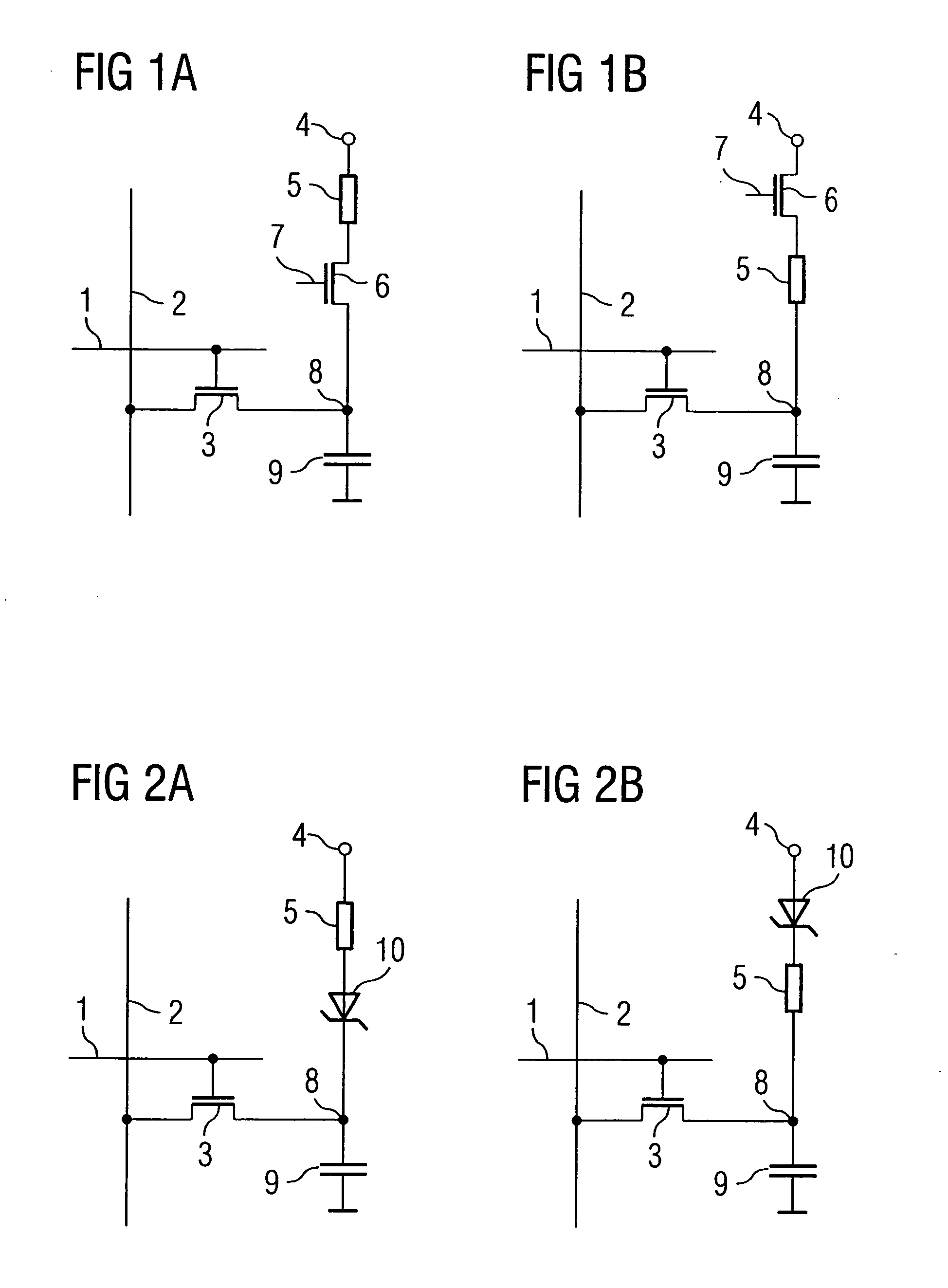
[0061] As is illustrated in FIGS. 2a and 2B, the second embodiment in which the polymer memory device 5 is coupled with a zener diode 10 may also be designed in two different variants that differ in the order of the diode 10 and the polymer memory cell 5. In the embodiment illustrated in FIG. 2A, the order of the series connection starts at the plate connection 4 with the polymer memory device 5 via the zener diode 10 to the capacitor 9. In the embodiment illustrated in FIG. 2B, the order of the series connection starts at the plate connection 4 with the zener diode 10 via the polymer memory device 5 to the capacitor 9. Depending on the layout or the optimization of the leaking current, the one or the other variant of the circuit may be preferred.

[0062]FIG. 11 shows an electric circuit for an inventive semiconductor memory according to the embodiment of the present invention illustrated in FIGS. 2A and 2B with a zener diode, wherein the semiconductor memory is designed according to ...

first embodiment

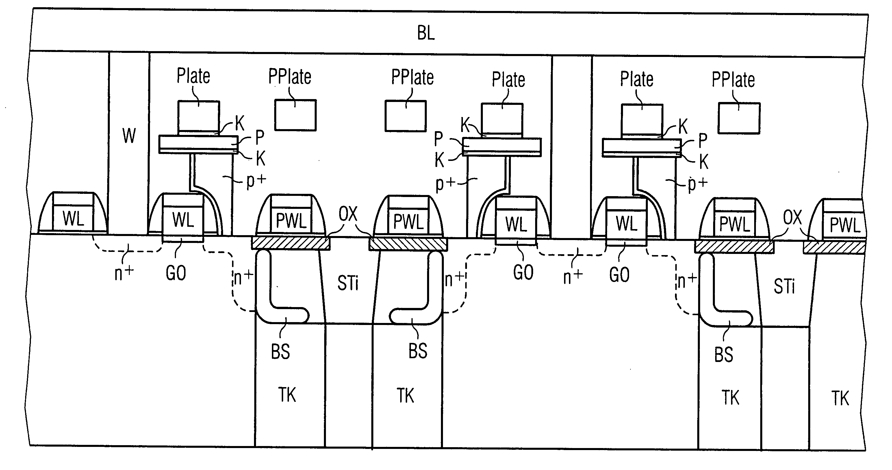
[0103]FIG. 13 shows an electric circuit diagram for a semiconductor memory according to the present invention with an additional transistor, wherein the semiconductor memory is designed according to the open bit line concept. The open bit line concept comprises a recurrent succession of electric lines that are arranged side by side and in parallel to each other in the following order:

[0104] word line WLi

[0105] control gate line CGi

[0106] plate line Platei

[0107] word line WLi+1

[0108] control gate line CGi+1

[0109] plate line Platei+1

[0110] These electric lines are crossed orthogonally by bit lines BLj and BLj+1. The volatile DRAM memory device comprises a word line transistor or selection transistor 3, respectively, and a capacitor 9, which are correspondingly controlled via the word lines WL and the bit lines BL. To this end, the word lines WLi+1 are connected with the gates of the selection transistors 3 while the bit lines are connected with the source / drain paths of the sele...


PUM


Abstract

The present invention relates to a semiconductor memory with a volatile memory device, in particular a DRAM memory device, and with a non-volatile memory device. The volatile memory device is electrically coupled with the non-volatile memory device, and the non-volatile memory device has a polymer memory device adapted to be switched between two states of information.

Description

CLAIMS FOR PRIORITY [0001] This application claims priority to German Application Nos. 10 2004 052 586.2 filed Oct. 29, 2004 and 10 2005 045 312.0 filed Sep. 22, 2005 which are incorporated herein, in their entirety, by reference. TECHNICAL FIELD OF THE INVENTION [0002] The invention relates to a semiconductor memory with a combination of volatile and non-volatile memory cells. The invention further relates to the operation, the design, and to differing layout concepts for a semiconductor memory with a combination of volatile memory cells and non-volatile polymer memory cells. BACKGROUND OF THE INVENTION [0003] A semiconductor memory device usually comprises a cell field consisting of a plurality of memory cells, and a matrix of column and line supply lines or word and bit lines, respectively. The memory cells are each positioned at the crosspoints of the electroconductive supply lines that are each electrically connected with the memory cell via an upper electrode or top electrode ...

Claims


Application Information

Patent Timeline
Patent Type & Authority Applications(United States)
IPC IPC(8): G11C11/24
CPCB82Y10/00G11C13/0009G11C13/0014G11C13/0016G11C14/00G11C14/0045H01L27/105H01L27/10897H01L27/286H01L51/0595H10B12/50H10K19/20H10K10/701
Inventor LIAW, CORVINWILLER, JOSEFKUND, MICHAEL
Owner INFINEON TECH AG
Why Eureka
Try Eureka