Multi-element phased array transmitter with LO phase shifting and integrated power amplifier

Active Publication Date: 2006-06-08
CALIFORNIA INST OF TECH
View PDF6 Cites 16 Cited by
  • Summary
  • Abstract
  • Description
  • Claims
  • Application Information

AI Technical Summary

Benefits of technology

[0013] The architecture of the multi-element phased-array transmitter (hereinafter alternatively referred to as transmitter) is adapted to provide flexibility to configure the transmitter as a two-dimensional 2-by-2 array or as a one dimensional 1-by-4 array. The transmitter uses a two step up-conversion architecture with an IF frequency of 4.8 GHz, in one embodiment. Double-quadrature architecture for the up-conversion stages attenuates the signal at image frequencies.
[0015] The phase selectors in each transmitter path have independent access to all the phases of the VCO. The double quadrature architecture results in two sets of phase selectors for each path, one for the in-phase (I) and one for the quadrature phase (Q) of the LO signal. The phase selection is done in two stages, with the first stage determining the desired VCO differential phase pair and the next stage selecting the appropriate polarity. The phase selectors can also be used as phase interpolators by selecting more than one phase pair at a time, thereby generating phases with resolution finer than 22.5°. The distribution of the multiple phases of the LO signal to the phase selectors in each path is carried out in a highly symmetric fashion to inhibit asymmetry in the LO signal. As is known, any asymmetry increases the power in the side-lobes, generates interference and clutter for radar and communication systems. Symmetric floorplanning and an H-tree based distribution structure ensure symmetry of the LO signals at each transmitter path. The configuration of the transmitter, including the beam-steering information is set through a digital serial interface.
[0016] The base band input signals I and Q drive a pair of double-balanced Gilbert type mixers in quadrature. The first set of mixers up-convert the base-band signal to 4.8 GHz. These mixers are followed by in-phase and quadrature signal buffers. An H-tree structure distributes the outputs of the 4.8 GHz buffers to the 4.8 GHz-to-24 GHz up-conversion mixers in each path. The outputs of the second up-conversion mixers are buffered and supplied to the PA driver. The cascode of tuned stages in the signal path increases the sensitivity of the transmitter to the frequency tuning of the passive tuned loads. Digitally switchable capacitors at the outputs of some of the high frequency tuned stages enable the adjustment of the center frequencies of these stages. The state of the switches is part of the initial digital calibration data loaded onto the chip.
[0017] Since all the circuits in the signal path up to, and including, the PA driver are differential while the two-stage PA is single-ended, an on-chip Balun is used for differential to single-ended conversion. The passive Balun is realized with a single-turn transformer to reduce substrate loss.

Problems solved by technology

As is known, any asymmetry increases the power in the side-lobes, generates interference and clutter for radar and communication systems.

Method used


Image

  • Multi-element phased array transmitter with LO phase shifting and integrated power amplifier
  • Multi-element phased array transmitter with LO phase shifting and integrated power amplifier
  • Multi-element phased array transmitter with LO phase shifting and integrated power amplifier

Examples


Embodiment Construction

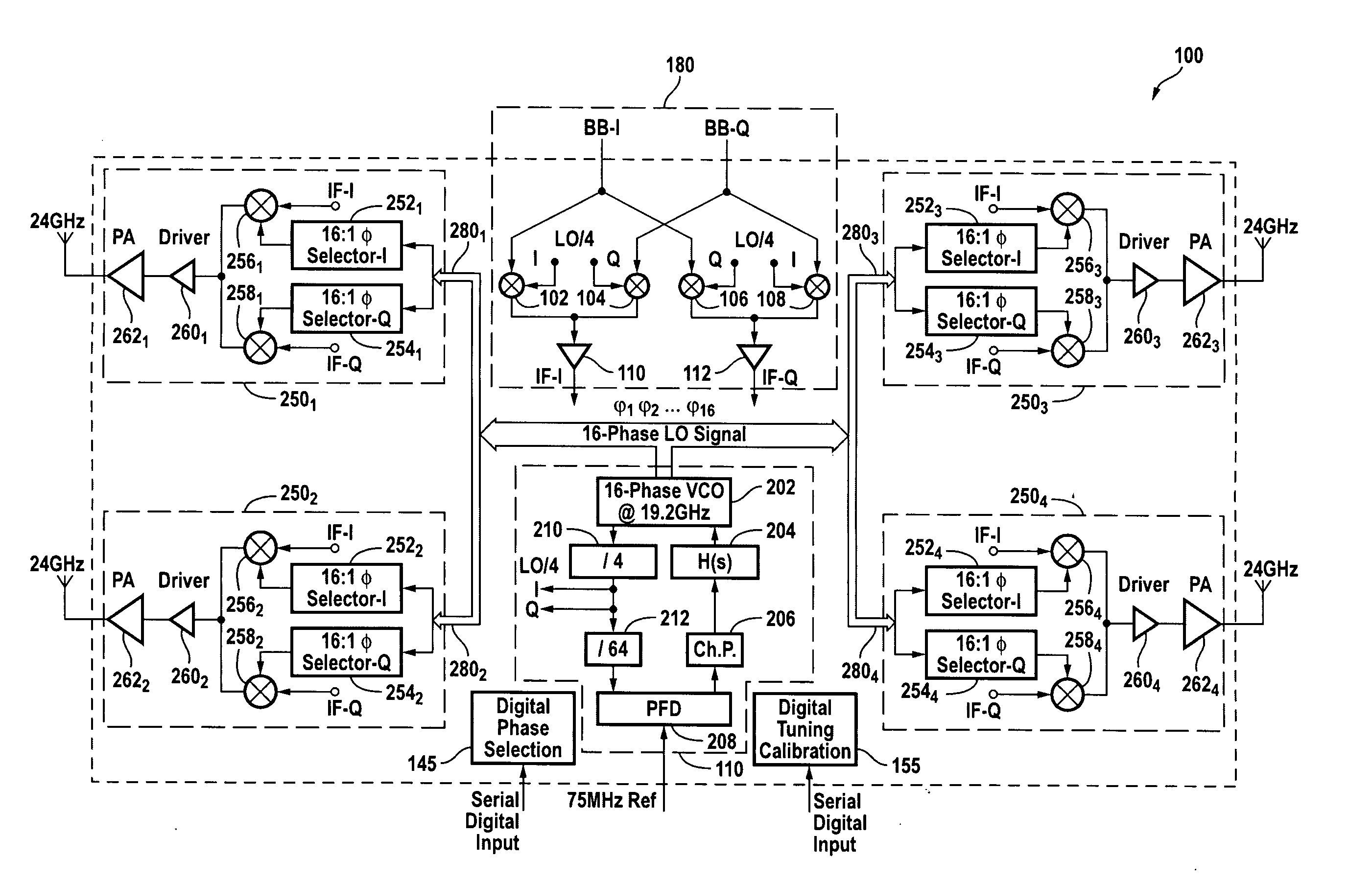
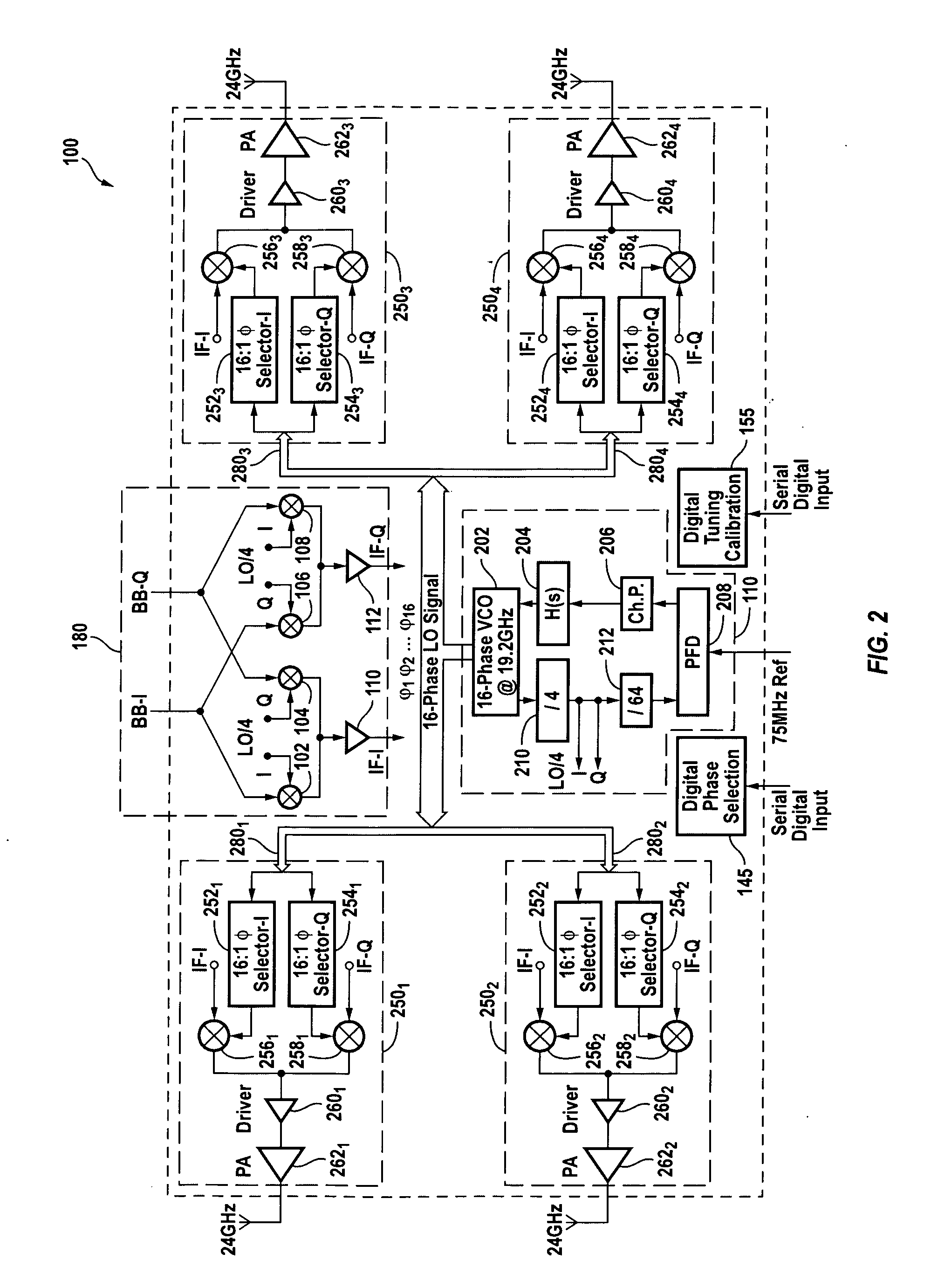
[0024] A fully integrated CMOS multi-element phased-array transmitter, in accordance with the present invention, includes, in part, on-chip power amplifiers (PA), with integrated output matching. In one embodiment, the phased-array operates at 24 GHz supporting bit rates of 500 Mb / s.

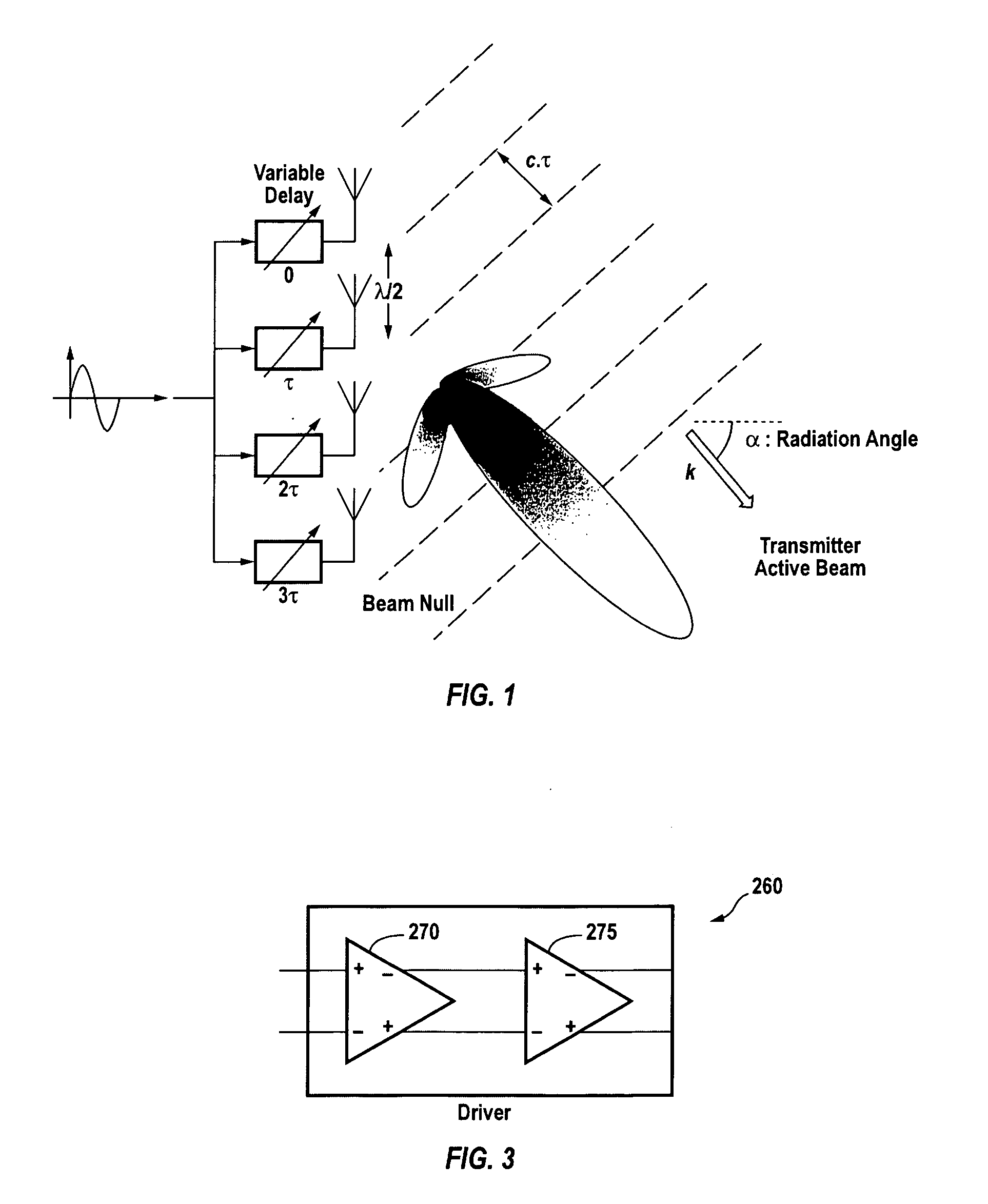
[0025]FIG. 2 is a high-level architecture and floorplan diagram of an exemplary multi-element phased-array transmitter 100, in accordance with one embodiment of the present invention. The architecture of the multi-element phased-array transmitter (hereinafter alternatively referred to as transmitter) 100 provides the flexibility to configure the transmitter as a two-dimensional 2-by-2 array or as a one dimensional 1-by-4 array. The transmitter uses a two step up-conversion architecture with an IF frequency of, for example 4.8 GHz in one embodiment. The double-quadrature architecture for the up-conversion stages attenuate the signal at image frequencies. A 16-phase CMOS VCO that includes eight differenti...


PUM


Abstract

A fully integrated CMOS multi-element phased-array transmitter (transmitter) includes, in part, on-chip power amplifiers (PA), with integrated output matching. The transmitter is adapted to be configured as a two-dimensional 2-by-2 array or as a one dimensional 1-by-4 array. The transmitter uses a two step up-conversion architecture with an IF frequency of 4.8 GHz. Double-quadrature architecture for the up-conversion stages attenuates the signal at image frequencies. The phase selectors in each transmitter path have independent access to all the phases of the VCO. The double quadrature architecture results in two sets of phase selectors for each path, one for the in-phase (I) and one for the quadrature phase (Q) of the LO signal. The phase selection is done in two stages, with the first stage determining the desired VCO differential phase pair and the next stage selecting the appropriate polarity. An on-chip Balun is used for differential to single-ended conversion.

Description

CROSS-REFERENCES TO RELATED APPLICATIONS [0001] The present application claims benefit under 35 USC 119(e) of U.S. provisional Application No. 60 / 614,390, filed Sep. 29, 2004 entitled “Multi-Element Phased Array Transmitted With LO Phase Shifting And Integrated Power Amplifier,” the content of which is incorporated herein by reference in its entirety. [0002] The present application is also related to co-pending U.S. application Ser. No. 10 / 988,199, filed Sep. 12, 2004, entitled “Monolithic Silicon-Based Phased Arrays For Communications And Radars,” the content of which is incorporated herein by reference in its entirety.BACKGROUND OF THE INVENTION [0003] The present invention relates to wireless communications, and in particular to a phased-array transmitter adapted for use in wireless communication systems. [0004] Omni-directional communication systems have been used extensively in various applications due, in part, to their insensitivity to orientation and location. Such systems, ...

Claims


Application Information

Patent Timeline
IPC IPC(8): H04B1/06
CPCH01Q3/22H01Q3/42
Inventor NATARAJAN, ARUNKOMIJANI, ABBASHAJIMIRI, SEYED ALI
Owner CALIFORNIA INST OF TECH
Why Eureka
Try Eureka